Download
1 / 20
210 likes | 416 Views
2005 updates to the Lithography chapter of the ITRS. Lithography International Technology Working Group July 2005. Lithography ITWG chair persons and co-chair persons for 2005. Summary of 2004 Lithography Chapter Updates.

E N D
2005 updates to the Lithography chapter of the ITRS Lithography International Technology Working Group July 2005
Lithography ITWG chair persons and co-chair persons for 2005
Summary of 2004 Lithography Chapter Updates • Defined more specific criteria for evaluating near-term potential solutions • Stronger emphasis on difficult challenges related to immersion lithography • Continued emphasis on challenges for implementing cost-effective post-optical lithography solutions
Proposed 2005 Lithography Updates • CD control and line edge roughness (LER) • Agreed along with Design, PIDS and FEP TWGs to increase CD tolerance to 12% • CD control for MPU gates is still red (red starts at <4 nm 3) • Agreed with FEP TWG on larger printed CD in resist • 1.6818physical gate length and 75%/25% variance allocation for lithography and etch, respectively • Proposed new definition of LWR and LER that better accounts for metrology, transistor and interconnect performance • Increased bias between size in resist and after etch for contacts • Significantly tighten overlay tolerances from 35% to 20% of DRAM ½ pitch • Add lithographic tool field width and length • Update potential solutions • Update colors and values in mask and resist tables Proposal only; Not for publication
2005 ITRS lithography requirements are challenging Update Update Proposal only; Not for publication
2005 updates to the chapter text • Table showing progression of low k1 methods • DFM section to complement content in Design chapter • Automatic process control (APC) detail • Cost of ownership factors and throughput factors described in text • Brief text about number of critical levels Proposal only; Not for publication
Criteria for potential solutions • All infrastructure (masks, tools, resist,…) needs to be in place to meet the ramp for the specified node • Technology must be planned to be used by IC makers in at least two geographical regions • For N+3 and later nodes with black coloring, the requirement to have more than one region support is not applicable • Technology should be targeting leading edge critical layer needs • Consideration (not a requirement): 100 tools worldwide over the life of that tool generation (not for each node)
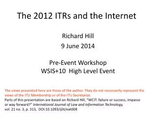
Lithography Potential Solutions Possible 2005 Update from Spring iTWG 2010 2019 2004 2007 2016 2013 2004 Lithography exposure tool potential solutions Technology Node hp90 hp65 hp45 hp32 hp22 hp16 Technology Options at Technology Nodes(DRAM Half-Pitch, nm) 90 193 nm DRAM Half-pitch(dense lines) 193nm 193i with water PEL? (decision by Sept.) RET = Resolution enhancement technology LFD = Lithography friendly design rules ML2 = Maskless lithography 65 193i with water 193i with other fluids EUV, ML2 EPL/PEL? (decision by Sept. 2005) 45 EUV 193i with other fluids and lens material Innovative 193i with water Imprint, ML2 32 EUV Innovative 193 nm immersion Imprint,ML2, innovative technology 22 Innovative technology Innovative EUV, imprint, ML2 16 Research Required Development Underway Qualification/Pre-Production Continuous Improvement Notes: RET and lithography friendly design rules will be used with all photon projection lithography solutions, including with immersion; therefore, it is not explicitly noted. Proposal only; Not for publication DRAFT – Work In Progress - NOT FOR PUBLICATION 13 July 2005
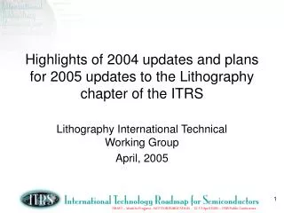
140 2001 Edition 2003 Edition 2005 Proposal 130@2001 120 100 90 90@2004 193nm+PSM 80 70 65@2007 193nm 60 PEL 50 PEL 45@2010 40 193nm+RET+LFD+Immersion PEL IPL PXL ? ML2 EPL? EUV EPL 32@2013 EPL 30 193nm Immersion 157nm+RET+LFD+Immersion EUV 193i w/ other fluids EUV ML2 ML2 Imprint Imprint 22@2016 20 +RET Innovation Innovation Innovation History of ITRS Litho Potential Solutions 248nm+PSM 157nm+PSM Acknowledge: Kameyama, Nikon
Significant changes to potential solutions in 2005 • 193nm immersion with water and other fluids expected to be primary technology through 45nm and perhaps 32nm ½ pitch with new lens materials • 157nm no longer seen as potential solution • EUV remains most likely next generation lithography (NGL) with possible use starting at 45nm ½ pitch and primary solution for 32nm and 22nm ½ pitch • Electron projection and proximity electron not as probable as in 2004 • Maskless lithography remains as potential solution starting at 45nm ½ pitch • Imprint extended to cover 32nm through 16nm ½ pitch Proposal only; Not for publication
Lens q Photoresist Silicon Wafer Resolution improvement by immersion Lens q Liquid Photoresist Silicon Wafer N water = 1.44
Enabling NA > 1.3 Numerical aperture 1.4 1.5 1.6 1.7 Water High Index Fluid Immersion Fluid High Index Lens Material Plano CaF2or SiO2 Final Lens Element Curved Final Element Existing Platforms High Index Resist Resist Earlier increase in index of fluid and/or resist yields process latitude improvement Acknowledge: Andrew Grenville
80 Ref. (%) 0 12.0 13.0 14.0 l (nm) Extreme Ultraviolet Lithography(EUV) Ring Field Illumination Scanning mask and wafer stages Flat, square mask with multilayers l = 13.5 nm Reflective Reticle Laser Produced Plasma All optics surfaces coated with multilayer reflectors (40 - 80 layer pairs, each layer approx l/4 thick, Control ~0.1 Å) Laser 40 Condenser Optics 4X Reduction Optics Wafer EUV imaging with ultrathin resist (UTR) 70nm 35nm Reflective Optical Surfaces are Aspheric with Surface Figures & Roughness < 3 Å
Device models Design rules Masks Designers Wafer fab Present mode of operation for circuit design and fabrication Layout Test data Packaged IC Circuit architecture Organizational, corporate cultural and geographical barriers
Device models Design rules Designers Wafer fab New mode of operation with design for manufacturing (DFM) practices Layout with critical paths Test data Packaged IC Circuit architecture Masks optimized based on design intent Statistical timing optimization Process variation distributions Known contours of CD, topography or overlay error with mfg. process
Proposed Changes to ITRS Resist Tables • Re-evaluated all colors in resist tables • Input from resist suppliers toward matching capability (colors) with requirements (numbers) • Re-examined defect size in resist films • Back surface particle levels updated based on FEP values • Improved LWR/LER definition and values Proposal only; Not for publication
Importance of Line Edge and Width Roughness Example: poly-silicon line • Line Edge Roughness (LER) (High frequency roughness) • Can affect dopant concentration profiles • Probably affects interconnect resistance • Line Width Roughness (LWR) (Mid-frequency roughness) • Leakage of transistors affected • Affects device speed of individual transistors • Leads to IC timing issues Edge assignment from SEM algorithm LWR LER Spatial frequency (nm-1) Ben Bunday, SEMATECH
Poly rs Rough Gate Edge Gate-SD Overlap disorder Gate n+ n+ Junction edge fluctuations Halo fluctuations Areas of potential device impact • Front end patterning • LWR after etch is what matters, not LWR in resist • LWR affects leakage current more strongly than drive current Fringing Field Disorder Nominal device w/o LER L=32nm Ioff ( nA / um on log scale ) L=40nm 7nm 3s LER L=50nm Ion ( uA / um ) Eric Verret, Aaron Thean and Jonathan Cobb; Freescale Semiconductor
Scaling relations for Table 77 and 79 ItemValue (in nm) where becomes: YellowRed CD = Physical gate width = 0.4 DRAM ½ pitch 40 20 Overlay = 20% DRAM ½ pitch 20 13 Minimum linewidth in resist = 1.6818 physical gate 50 25 Contact size after etch = 1.125 ½ pitch 85 60 Contact in resist = 1.1 contact after etch 85 60 CD control for DRAM = 13.5% sqrt(0.75) DRAM ½ pitch 7 4 CD control for MPU/ASIC = 7 4 12% sqrt(0.75) MPU/ASIC M1 contacted ½ pitch Mask nominal image size = MAG resist linewidth 200 130 SRAF feature is ½ of mask nominal image 130 100 Mask Min. Primary Feature Size = 200 130 0.7 Mask nominal image size Mask CD control = CD MAG sqrt(0.75) 4% / MEEF 8 5 Placement = Overlay MAG 15% 14 10 Defect size = DRAM ½ Pitch MAG / 5 80 60 Linearity = 3.8% DRAM ½ pitch MAG 15 10 CD mean-to-target = 2% DRAM ½ pitch MAG 7 4 Absorber LER = Min. CD MAG 3% 7 4 Blank flatness 1/NA2 (250nm in 2007) 250 150 Data volume = 2 increase / node (260 GB in 2004) 260 5000 GB Update Proposal only; Not for publication DRAFT – Work In Progress - NOT FOR PUBLICATION 13 July 2005
Summary • 193nm immersion and EUV lithography are promising candidate technologies for 45-nm and 32-nm half-pitch patterning • Significant challenges remain in developing either technology to provide a timely, economical manufacturing solution • Innovations in immersion, EUV and new techniques such as ML2 and imprint might become prevalent starting at 32-nm ½ pitch • Maintaining ±10% CD control doesn’t appear to be possible, and ±12% adopted, ±12% still difficult to achieve • More stringent overlay tolerances important for manufacturing of memory circuits • Measuring and controlling LWR and LER becoming increasingly important • Increasing integration of design, modeling, lithographic resolution enhancement techniques and extensive metrology will be needed to maintain expected circuit performance