Download
1 / 26
260 likes | 408 Views
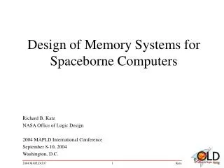
Design of Memory Systems for Spaceborne Computers. Richard B. Katz NASA Office of Logic Design 2004 MAPLD International Conference September 8-10, 2004 Washington, D.C. Agenda.

E N D
Design of Memory Systems for Spaceborne Computers Richard B. Katz NASA Office of Logic Design 2004 MAPLD International Conference September 8-10, 2004 Washington, D.C.
Agenda This seminar will discuss the design of memory systems for spaceborne computers. While normally associated with computers, many of the concepts in this seminar also apply to the "configuration memory" of FPGAs. The seminar will include a discussion of the following topics: • Memory classification • Review and discussion of spaceborne memory system architectures in both manned and robotic NASA missions • Robust memory system design and criteria • Impact of software on memory system integrity • Frequently seen problems and lessons learned • Component considerations - Cell and device failures - Lock up • Recommendations
Memory Classification • While normally associated with computers, many of the concepts in this paper also apply to the “configuration memory” of FPGAs. • Fixed • The contents of the memory are physically fixed by the structure of the memory element. • Examples: core rope memories (wire wound through or around a core), fusible link PROMs, and antifuse-based PROMs. • Erasable • The contents of the memory are non-volatile, like the fixed memories, but the contents can be changed. In many cases this involves an erase operation and then a write. • Examples: core, plated wire, electrically erasable programmable read only memories (EEPROM), erasable read only memories (EPROM), ferroelectric memories, and flash. The “ROM” in EPROM and EEPROM is a poor part of the name as it implies permanence, which is incorrect. Devices such as EEPROM may need “refreshing” over long missions as many are rated with a 10 year storage lifetime, giving them dynamic characteristics. • Volatile • The contents of the memory are volatile; they do not retain contents either after the cycling of power or during “brown out” conditions. This class is subdivided into two subclasses, static, which will retain state indefinitely and dynamic, where the memory must be read and subsequently refreshed. • Examples include SRAM, DRAM, and SDRAM.
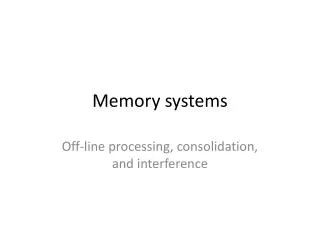
Memory A Memory B Error Detect Logic Error Detect Logic Buffer Register A Buffer Register B Memory Select Logic From Processor To Processor From Processor Saturn V Launch Vehicle Duplex Memory Each of the two core memory units was accessed in parallel and each contained parity. If an error was detected in the memory unit currently designated as prime, then data from the secondary unit was used with the secondary unit now given the prime designation. Hardware automatically wrote corrected data upon the detection of an error.
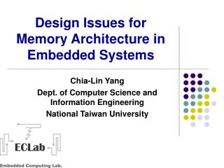
Simplified block diagram of the Apollo Guidance Computer (AGC) Apollo Guidance Computer The advantages of the ropes are numerous. The program, once wired in, cannot be electrically altered, a substantial asset for mission reliability. [2] The permanent memory requires very few active components and very little power to operate, It also has properties that make it indestructible short of mechanical damage, that is, there is no inflight failure of any kind that can destroy this part of the memory. … In case of inflight failure that destroys the information in this [erasable] memory the computation can be restarted by reading in only a very few words. [3]. Memories in the AGC were single string; each memory used a parity bit for error detection. “Fixed storage” was core rope, a permanent memory technology, with coincident current core implementing erasable memory. “Involuntary instructions,” which operated as an interrupt and not under program control, could shift data into specific words of memory. Data could also be entered via the astronauts’ keyboard and the the "PACE" digital command system before launch. [3]
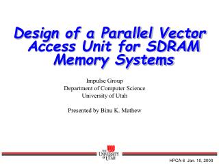
Interface Interface Processor Processor Galileo Attitude Control Computer RTG Power For Keep-A-Live RTG Power For Keep-A-Live CMOS Memory Array CMOS Memory Array ROM ROM GSE/DMA GSE/DMA Arbiter/ Controller Arbiter/ Controller C&DH/DMA C&DH/DMA Memory units were accessed one at a time. There was no parity and RAM contents were protected by write protect registers and monitored by checksums in the background. Primary and secondary memory designs were switched via a discrete command. ROM contents implemented safe-hold mode. DMA was functional either with the processor clamped in reset or executing flight software. A “heartbeat” was sent to the C&DH via DMA.
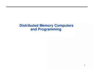
Single String Computer A Single Board Computer Conceptual diagram. Code redundantly stored in three EEPROM modules. Switching between copies is implemented in software and all software must be running to be able to accept and process the command to switch images. The critical boot code and interrupt vectors can not be made fault tolerant in this software-centric architecture. Command to the flight software. µP Logic Device Simplified software-centric architecture. Switching between critical boot sections is done by software, leaving single point failures in this architecture. There is no parity or EDAC. Boot Code Boot Code Boot Code EEPROM Module #1 EEPROM Module #2 EEPROM Module #3
Logic Device Logic Device Single String Computer B These two computers are based on the same base SBC but reflect different engineering approaches. Single Board Computer Conceptual diagram. Code redundantly stored in three EEPROM modules. Switching between copies is implemented in hardware by an external discrete command. µP Hardware command selects between one of two spare modules. Hardware command for either on- or off-board boot code selection. Simplified hardware-centric architecture. Switching between critical boot sections is done by hardware discretes, eliminating the EEPROM as a single point failure. Common mode EEPROM failure modes do remain. Boot Code Boot Code Boot Code EEPROM Module #1 EEPROM Module #2 EEPROM Module #3
Science Data Interface Pattern Generators (Algorithmic and Table-Based) ROM RAM RAM EEPROM uP PROM Memory Controller TLM Processor CMD Processor S/C Telemetry S/C CMD Time Sync Lunar Orbiter Laser Altimeter (Proposed) Block diagram of proposed processing electronics. S/C CMD and telemetry interfaces can read and write all memory locations directly; the processor may be clamped in reset for these operations. The microprocessor may boot to safe-hold from on-chip ROM or RAM or off-chip PROM, EEPROM, or RAM. Default science algorithms are stored in PROM with the EEPROM providing operational flexibility for new algorithms that are uploaded.
Requirement: Design Against Any Credible Off-Nominal Event These Events Are Considered Both Credible and Likely: • Power Transitions and Disruptions • Power Up Transient • Power Down Transient • “Glitches” or brownouts on power lines • Software Faults • Cell and Device Failure • Asynchronous Reset
Power Transitions and Disruptions • Three Cases • Power Up Transient • Power Down Transient • “Glitches” or brownouts on power lines • Many designers use a simple RC timing circuit for the generation of a POR or “Power On Reset” signal. Looking closely at the acronym, is has the word “on” in it and the “O” does not stand for “Off.” • The RC timing circuit will result in a signal that has lag and will not be asserted early to protect erasable memory contents during power down and transients. (cont’d on next slide)
Power Transitions and Disruptions (cont’d) • Reset circuit characteristics • Power-on: Assert early and hold until after all voltages and circuits are stable • Power-off: Assert prior to the removal of power • “Glitches” and brown-outs: Similar to the power-off Case. • Often best generated in the power supply • Carefully analyze the signals controlling the memories • Controls are often implemented by an FPGA that is not guaranteed to be under control during the power-on, power-off, and periods when power is disrupted. FPGA and configuration memory device internal power-on reset circuits may be active along with initialization sequences, charge pumps have to supply sufficient charge and voltage to turn on high-voltage isolation FETs, etc. • Erasable memory device protection is an analog function and digital components must be used with extreme care. Along with timing, many memory devices require non-standard voltage levels and currents for protection.
Software Faults • Consider the likelihood of a software fault is 100%. • Device Protection • Many erasable devices implement “software write protection” to prevent against inadvertent writes to the memory. • JEDEC has published a standard on this type of protection. • Do not keep the “keys” to unlock the memory on-board unless absolutely necessary. • Subsystem Protection • System level write protection limits, implemented in hardware, to protect against software faults. • Some systems implement this in software which is risky; see bullet #1 above. • Use external hardware discrete command as an additional barrier to prevent inadvertent writes.
Cell and Device FailureGeneral Guidelines to be Tailored for Each Mission and Application • High-reliability, radiation-hardened CMOS RAM and PROM is available. • Designing against cell and device failure should be consistent with mission rules on single point failures. • Examine “radiation-hardened” label carefully as some devices marked as such are in fact SEU soft. • Commercial off the shelf (COTS) and Single Event Upset (SEU) soft devices should have parity for error detection or error detection and correction (EDAC) circuits, as required for the application. • Analyze and test devices for lockup states. These can occur in many memory types from illegal loads into command registers, poor signal integrity, poor power quality, or an SEU. Some device lockup states require power cycling to clear. • Consider the likelihood of an EEPROM or flash device fault to be 100%. There are enough failures in the industry to justify such an approach.
Asynchronous Reset • Consider the system effects on the memory subsystem from an asynchronous reset. • Power disruption as discussed above, which are included here. • Reset either from another on-board computer or a ground command, perhaps in an attempt to clear a fault. • Will write cycles be aborted while being setup or in-process, leaving a non-volatile memory in an undefined state or altering RAM contents from a warm boot no longer valid? • Hardware memory controllers • Flight software, which is often involved by some systems in generating sequences and timing for non-volatile memories. • Will hardware operations be given time and energy to complete on-going operations? Many non-volatile memory devices take on order of 10 ms to complete.
Frequently Seen Problems • Reset signals to memory devices not properly driven. • Higher current requirements are frequently ignored, resulting in too large of a voltage drop across a “pull-up resistor.” • Non-standard logic thresholds are frequently ignored, resulting in too small of a DC noise margin. • The two issues above, either singly or in concert, can result in the device going into a protection mode and not operating, causing memory fetch operations to fail and present incorrect data on a byte-wide basis to a CPU. • Power-off and brown out electrical conditions are often ignored. Non-volatile memories are not protected. • Device internal write protection not used. • FPGAs provide control of the non-volatile memory devices: • FPGA transient behavior not understood or considered • FPGA state machine response to SEUs not considered. (cont’d on next slide)
Frequently Seen Problems • Non-volatile, erasable memories are used for boot and safe hold. • Risky in general as there is no fixed memory. Many implementations are single string. • Risky in particular since there are a lot of unexplained failures in the industry. • Software architectures require that entire computer systems, hardware and software, be operational to accept any commands. Thus, if there are any problems, there is often little or nothing that can be done from the ground. • Lockup states in memory devices are often not considered either in memory controller designs (soft resets) or system designs (power cycle required for clearing of faults). • Critical switching between memory images for booting implemented as a software function which can not be guaranteed to function under all credible faults resulting in system lockup. (cont’d on next slide)
Frequently Seen Problems • DMA functions require software to be operational to initiate transfers which can not be guaranteed to function under all credible faults. • Technology often not understood. For example, some memory devices while logically permitting byte writes, only perform subpage writes, resulting in an incorrect count of write cycles per location, with many erasable memory technologies being write cycle limited.
Some Component ConsiderationsNon-volatile Memory “Lockup” “SEFI” data for the R1701L PROM This “stuck at” mode, not necessarily 0, requires power cycling of this serial device to clear. [5] See also [6] and other reports for similar results. t SEE Test Results for AT28C010 (EEPROM) [4] Types I and II are Single Effect Functional Interrupts (SEFI) and required power cycling to restore functionality. Errors can be multi-bit, defeating SEC/DEC EDAC schemes. Some but not all non-volatile memory components can enter lockup states and become “stuck,” requiring the cycling of power to restore functionality. Careful system considerations for the use of such devices is needed, with regards to error detection and clearing, protection of device I/O pins, and loss of system functionality and propagation of errors until recovery is achieved.
10-3 10-4 10-5 10-6 10-7 Cross-section (cm2/device) LET (MeV-cm2/mg) Some Component ConsiderationsSynchronous DRAM (SDRAM) “Lockup” BURST LENGTH A2 A1 A0 M3=0 M3=1 0 0 0 1 1 0 0 1 2 2 0 1 0 4 4 0 1 1 8 8 1 0 0 RESERVEDRESERVED 1 0 1 RESERVED RESERVED 1 1 0 RESERVED RESERVED 1 1 1 FULL PAGE RESERVED Loss of functionality for the Hyundai 256M SDRAM (Auto Refresh Operation Mode) [7] Examination a command field, Burst Length, for a Load Mode Register command for one SDRAM type. SDRAMs contain finite state machines and some models may lock up, requiring the cycling of power, if RESERVED commands are loaded. For some models, this can result in potential damage to a device. Other methods of entering illegal and potentially damaging states is via an SEU, as shown in the chart on the right, and error in the controlling device, poor signal integrity or poor power quality. Careful system considerations for the use of such devices is needed, with regards to error detection and clearing, spare replacement devices in the event of damage, and loss of system functionality and propagation of errors until recovery is achieved.
Recommendations • Boot and Safe-Hold Code: • High-reliability, radiation-hardened, fixed memories should normally be employed for boot and safe-hold functions. • For applications such as instruments, DMA functions, properly implemented, can load memories with boot code. In this case, the instrument should be safed by hardware logic. • DMA functions should not require any operational software. A hardware discrete command to clamp a processor into reset is also recommended. • Hardware discrete commands should be used for switching critical memory banks, not software. • Checking Memory Validity • Parity should be used as practical. • CRC or block parity is useful for the storage of frames or blocks of data. • Checksums should be run in the background during idle time. (cont’d on next slide)
Recommendations • Lockup States Must Be Considered • Select devices that do not have lockup states, if possible. • No device with a lockup state should be mission-critical or safety-critical. • Memory controllers should be tolerant of these conditions and at a minimum attempt to clear lockup states in devices • System devices should be tolerant of these conditions and be able to cycle power to clear those lockup states that require power cycling while meeting all mission requirements. • Systems should require the minimum of resources to function to enhance the probability of survival in the presence of either faults or off-nominal events. • Erasable memory devices should permit an analog measurement of state of a bit. For example, for an EEPROM cell, the amount of charge on the cell should be represented by an analog signal that is digitized. This enables margins to be determined and trends to be measured, detecting “weak cells” or other problems as early as practical during test. (cont’d on next slide)
Recommendations • Erect Barriers to Prevent Inadvertent Contamination of Erasable Memory Contents • Write protection registers implemented in hardware to prevent software errors from corrupting memory contents • Use device specific protection functions such as “memory protect” hardware pins and required software sequences to restrict writes. Do not store software keys on board but make part of a command and not core software. • Select erasable memory devices that are not self-contained. That is, if a clock signal and high voltage are required to alter the memory contents, they should not be generated on-chip but at the system level. This permits the logic designer to insert barriers between the logic signals required to write (clock signals) and energy source (high voltage) and the memory device. • “Refreshing” of critical code, such as boot code, that is stored in erasable memory should not be done to mitigate faulty devices. Instead, use reliable fixed memory technology. (cont’d on next slide)
Recommendations • Verify Margins of All Protection Signals • DC voltage margin • AC voltage margins (e.g., cross talk) • Timing (protection signals for power up, power down, and during glitches). The power down rate of voltage buses is often ignored or idealized. • Ensure that all in process, critical write cycles have time to complete properly. • Consideration of effects and propagation of logical resets • Ensuring enough energy is in the system to permit write cycles to properly finish before the voltage is out of specification. • Third party device packaging houses • Verify that they fully understand the technology and the original manufacturer’s test procedures and screening criteria • Compare failure rates of third party houses with those reported by the original die manufacturer • Ensure that proper and complete testing for space missions is performed (cont’d on next slide)
Recommendations • Understand All Failure Modes and Consider Common Mode Failures and their system effects. • Certain models EEPROM, flash, DRAM, and SDRAM have been seen to have various lockup modes or test modes that can be entered by credible, off-nominal events. • Non-hardened SRAM, DRAM, SDRAM, etc., can have “stuck bits” from radiation. • Multiple copies of the same code in the same technology is risky, if the fundamental technology is not reliable. With the current rash of industry failures of EEPROM, for example, multiple copies of the same device type, even with hardware selection, is a form of Russian Roulette. Storing redundant copies of code in separate blocks of one device can be subject to common mode failures. • Treating bit, block, and device failures in software can be done in many instances, such as recorders. For critical boot code, as an example, treating failures as a software maintenance issue that must be done before a reset, should not be a function relegated to software. That would be a form of “foam logic.”
References • Space Vehicle Design Criteria, (Guidance and Control): Spaceborne Digital Computer Systems, NASA SP-8070, March 1971, National Aeronautics and Space Administration • “The Apollo Guidance Computer,” Ramon L. Alonso and Albert L. Hopkins, R-416, August, 1963. • “General Design Characteristics of the Apollo Guidance Computer,” Eldon C. Hall, R-410, May 1963. • “Single Event Functional Interrupt (SEFI) Sensitivity in EEPROMs,” R. Koga, 1998 MAPLD International Conference, September, 1998, Greenbelt, MD. • “Single-Event Upset Test Results for the Xilinx R1701L PROM,” S. M. Guertin, JPL Report, August 24, 2000 • “SEE and TID Extension Testing of the Xilinx XQR18V04 4Mbit Radiation Hardened Configuration PROM,” Carl Carmichael, Joe Fabula, Candice Yui, and Gary Swift, 2002 MAPLD International Conference, September 10-12, 2002, Laurel, MD. • "Permanent Single Event Functional Interrupts (SEFIs) in 128- and 256-megabit Synchronous Dynamic Random Access Memories (SDRAMs)," R. Koga, P. Yu, K.B. Crawford, S.H. Crain, and V.T. Tran, 2001 IEEE Radiation Effects Data Workshop.