8255 Programmable Peripheral Interface
Learn about the MPU interface to external devices, parallel and serial data transfer modes, I/O pins, control words, and communication steps with examples. Explore modes 0, 1, and 2 for different functionalities.


8255 Programmable Peripheral Interface
E N D
Presentation Transcript
Introduction • MPU interface to external devices through both parallel and serial interfaces. • Parallel data occur in system that use: • Displays • Keyboard • Printers (old printer) • Etc. • Serial data occurs in: • Some printers • Data communications
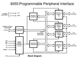
About • 24 I/O pins • 8 bit parallel ports: A, B • C port: can be grouped as 4 bit CU(C upper) and CL(C Lower) • Two Modes: BSR(Bit Set/reset) and I/O mode • BSR mode set/reset in port C • I/O mode is further divided in 3 modes: • Mode 0: simple • Mode 1: Handshake • Mode 2 : Bidirectional
Function of pins: • Data bus(D0-D7):These are 8-bit bi-directional buses, connected to 8085 data bus for transferring data. • CS: This is Active Low signal. When it is low, then data is transfer from 8085. • Read: This is Active Low signal, when it is Low read operation will be start. • Write: This is Active Low signal, when it is Low Write operation will be start.
Function of pins: • Address (A0-A1):This is used to select the ports. like this
Function of pins: • RESET: This is used to reset the device. That means clear control registers. • PA0-PA7:It is the 8-bit bi-directional I/O pins used to send the data to peripheral or to receive the data from peripheral. • PB0-PB7:Similar to PA • PC0-PC7:This is also 8-bit bidirectional I/O pins. These lines are divided into two groups. • PC0 to PC3(Lower Groups) • PC4 to PC7 (Higher groups) These two groups working in separately using 4 data’s.
Control Word • Can be accessed when A0=1 and A1=1 • Cannot be accessed for read operation • Steps to communicate with 8255 • Determine the addresses of port A,B and C and control register according to CS and A0 ,A1 • Write control word in control register • Write I/O instruction to communicate with peripheral through A,B and C
Mode 0: Simple Input or Output • In this mode, ports A, B are used as two simple 8-bit I/O ports and port C as two 4-bit ports. Each port can be programmed to function as simply an input port or an output port. The input/output features in Mode 0 are as follows. • Outputs are latched. • Inputs are not latched. • Ports don’t have handshake or interrupt capability.
Figure 9: • Example :
8255 PIA: Example • Solutions: • Port Address : • It is actually an I/O memory map. • When A15 is active high, Chip Select signal is activated. • Assuming all don’t care signals are at logic 0, therefore ports’ address are as follows:
8255A Programmable Peripheral Interface • Solution: • Control Word:
8255 PIA • Solution: ???
Mode 1: Input or Output with Handshake • In this mode, handshake signals are exchanged between the MPU and peripherals prior to data transfer. The features of the mode include the following: • Two ports (A and B) function as 8-bit I/O ports. They can be configured as either as input or output ports. • Each port uses three lines from Port C as handshake signals. The remaining two lines of Port C can be used for simple I/O operations. • Input and Output data are latched. • Interrupt logic is supported.
Signal Description • STB- Strobe input: (active low) : generated by peripheral to indicate it has transmitted the data. • IBF( Input buffer full) : Acknowledged by 8255 to indicate the input buffer has received the data. • INTR( Interrupt Request) : This is output signal that is used to INTR the uP. This is high when STB , IBF and INTE(internal signal) is high. Means the 8255 is processing the data. • INTE (Interrupt Enable): internal flip flop
82C55: Mode 2 Bi-directional Operation • This functional configuration provides a means for communicating with a peripheral device or structure on a single 8-bit bus for both transmitting and receiving data (bidirectional bus I/O). • “Handshaking” signals are provided to maintain proper bus flow discipline in a similar manner to MODE 1. • Interrupt generation and enable/disable functions are also available.
MODE 2 Basic Functional Definitions: • Used in Group A only. • One 8-bit, bi-directional bus port (Port A) and a 5-bit control port (Port C). • Both inputs and outputs are latched. • The 5-bit control port (Port C) is used for control and status for the 8-bit, bi-directional bus port (Port A).
82C55: Mode 2 Bi-directional Operation • INTR : Interrupt request is an output that requests an interrupt. • ~OBF : Output Buffer Full is an output indicating that that output buffer contains data for the bi-directional bus. • ~ACK : Acknowledge is an input that enables tri-state buffers which are otherwise in their high-impedance state. • ~STB : The strobe input loads data into the port A latch.
82C55: Mode 2 Bi-directional Operation • IBF : Input buffer full is an output indicating that the input latch contains information for the external bi-directional bus. • INTE : Interrupt enable are internal bits that enable the INTR pin. BIT PC6(INTE1) and PC4(INTE2). • PC2,PC1,PC0 : These port C pins are general-purpose I/O pins that are available for any purpose.
82C55: Mode 2 Bi-directional Operation • Timing diagram is a combination of the Mode 1 Strobed Input and Mode 1 Strobed Output Timing diagrams.
Mode 2: Bidirectional Data Transfer • This mode is used primarily in applications such as data transfer between two computers. In this mode, Port A can be configured as the bidirectional port and Port B either in Mode 0 or Mode 1. • Port A uses five signals from Port C as handshake signals for data transfer. The remaining three signals from port C can be used either as simple I/O or as handshake for port B.
BSR (Bit Set/Reset) Mode • The BSR mode is concerned only with the eight bits of port C, which can be set or reset by writing an appropriate control word in the control register. • A control word with bit D7 =0 is recognized as a BSR control word, and it does not alter any previously transmitted control word with bit D7=1; thus the I/O operations of ports A and B are not affected by a BSR control word. • In BSR mode, individual bits of port C can be used for applications such as an on/off switch. Ports A and B are not affected by the BSR Mode.
8255 PIA: BSR Mode • Example: • Write a BSR control word subroutine to set bit PC7 and PC3, and reset after 10ms. Use the schematic diagram as shown below.
8255A Programmable Peripheral Interface • Solution: • BSR Control Word: • Port Address: • As shown in previous example : 83H
8255A Programmable Peripheral Interface • Solution: • Subroutine: Assuming that the delay subroutine has been determined earlier.