Download
1 / 46
460 likes | 535 Views
Learn how x86 CPUs access I/O space using I/O ports, Understand I/O instructions like IN and OUT, Master interfacing with 8255 chip, Explore 8-bit and 16-bit I/O operations, Implement I/O instructions in programming.

E N D
I/O AND THE 8255; ISA BUS INTERFACING Chapter 11
In addition to memory space, x86 microprocessors also have I/O space. This allows it to access ports. • What is the function of ports?
Ports are used to • bring data into the CPU from an external device such as the keyboard or • send data from the CPU to an external device such as a printer.
8088 INPUT/OUTPUT INSTRUCTIONS • All x86 microprocessors, from the 8088 to the Pentium, can access external devices called ports using I/0 instructions. • The x86 CPU is one of the few processors that have I/O space in addition to memory space. • Memory can contain both opcodes and data • I/O ports contain data only. Two instructions: “OUT” and “IN”. • These instructions can send data from the accumulator (AL or AX) to ports or bring data from ports into the accumulator. • In accessing ports, we can use an 8-bit or 16-bit data port.
8-bit data ports • The 8-bit I/O operation of the 8088 is applicable to all x86 CPUs from the 8088 to the Pentium. • The 8-bit port uses the D0 - D7 data bus to communicate with I/O devices. Instructions OUT and IN have the following formats: Inputting DataOutputting Data Format: IN dest, source OUT dest,source • IN AL,port# OUT port#,AL (2) MOV DX,port# MOV DX,port# IN AL,DX OUT DX,AL
Inputting DataOutputting Data Format: IN dest, source OUT dest,source • IN AL,port# OUT port#,AL • port# is the address of the port and can be from 00 to FFH. • This 8-bit address allows 256input ports and 256 output ports. • In this format, the 8-bit port address is carried on address bus A0 - A7.
Format: Inputting DataOutputting Data (2) MOV DX,port# MOV DX,port# IN AL,DX OUT DX,AL • port# is also the address of the port, except that it can be from 0000 to FFFFH, allowing up to 65,536 input and 65,536 output ports. • The 16-bit port address is carried on address bus A0 – A15 • The use of a register as a pointer for the port address has an advantage in that the port address can be changed very easily, especially in cases of dynamic compilations where the port address can be passed to DX.
16-bit data ports • Instructions OUT and IN have the following formats: Inputting DataOutputting Data Format: IN dest, source OUT dest,source • IN AX,port# OUT port#,AX (2) MOV DX,port# MOV DX,port# IN AX,DX OUT DX,AX
How to use I/O instructions • I/O Instructions are widely used in programming peripheral devices such as printers, hard disks, and keyboards. The port address can be either 8-bit or 16-bit. • For an 8-bit port address, we can use the immediate addressing mode. The following program sends a byte of data to a fixed port address of 43H. MOV AL,36H ;AL=36H OUT 43H,AL ;send value 36H to port address 43H
8-bit address 256 input or outputports. • 16-bit address larger number of ports. • To use the 16-bit port address, register indirect addressing mode must be used. The register used for this purpose is DX. • The following program sends values 55H and AAH to I/O port address 300H (a 16-bit port address); the program toggles the bits of port address 300H continuously. BACK: MOV DX,300H ;DX = port address 300H MOV AL,55H OUT DX,AL ;toggle the bits MOV AL,0AAH OUT DX,AL ;toggle the bits JMP BACK
We can only use register DX for 16-bit I/O addresses. Also notice the use of register AL for 8-bit data. • The following code transfers the contents of register BL to port address 378H. MOV DX,378H ;DX=378 the port address MOV AL,BL ;load data into accumulator OUT DX,AL ;write contents of AL to port ;whose address is in DX • To bring into the CPU a byte of data from an external device (external to the CPU) we use the IN instruction; see Example 11-1.
Example 11-1: In a given 8088-based system, port address 22H is an input port for monitoring the temperature. Write Assembly language instructions to monitor that port continuously for the temperature of 100 degrees. If it reaches 100, then BH should contain ‘Y’. Solution: BACK: IN AL,22H ;get the temperature from port # 22H CMP AL,100 ;is temp = 100? JNZ BACK ;if not, keep monitoring MOV BH,’Y ;temp = 100, load ‘Y’ into BH
The following program gets data from port address 300H and sends it to port address 302H. MOV DX,300H ;load port address IN AL,DX ;bring in data MOV DX,302H OUT DX,AL ;send it out
ADDRESS DECODING AND DESIGN • We’ll see the design of simple I/O ports using TTL logic gates 74LS373 and 74LS244. • The concept of address bus decoding for I/O instructions is exactly the same as for memory. The following are the steps: 1. The control signals IOR and lOW are used along with the decoder. 2. For an 8-bit port address, A0 – A7 is decoded. 3. If the port address is 16-bit (using DX), A0 - Al5 is decoded.
74LS373 In an output port design • In every computer, whenever data is sent out by the CPU via the data bus, the data must be latched by the receiving device. • While memories have an internal latch to grab the data, a latching system must be designed for simple I/O ports. • The 74LS373 can be used for this purpose.
74LS373 In an output port design • Analyze Figure 11-2. Under what condition(s) 74LS373 is activated? Figure 11-2. Design for “OUT 99H,AL”
IN port design using the 74LS244 • When data is coming in by way of a data bus, it must come in through a three-state buffer. • This is referred to as tristated, which comes from the term tri-state buffer. • “tri-state” is a registered trademark of National Semiconductor Corp.
The design of an output port with an address of 31FH using the 74LS373 is shown below. 0 px Design for Output port address of 31FH
A tri-state buffer is internal and therefore invisible. • For the simple input ports we use the 74LS244 chip. See Figure 11-4. • Notice that since 1G and 2G each control only 4 bits of the 74LS244, they both must be activated for the 8-bit input Figure 11-4. 74LS244 Octal Buffer
Problem. What change(s) would you do to change the design to “IN AL,6AH”?
Memory Mapped I/O • Communicating with I/O devices using IN and OUT instructions is referred to as peripheral I/O or isolated I/O. • However, there are many microprocessors, such as the new RISC processors, that do not have IN and OUT instructions. • In such cases these microprocessors use what is called memory-mapped I/O. • In memory-mapped I/O, a memory location is assigned to be an input or output port.
The design of “IN AL,9FH” using the 74LS244 as a tri-state buffer is depicted below.
I/O ADDRESS MAP OF X86 PCS • Designers of the original IBM PC decided to make full use of I/O instructions. • The list of the designated I/O port addresses is referred to as the I/O map;seeTable 11-1. A much more detailed I/O map of the x86 PC is given in Appendix G. • Any system that needs to be compatible with the x86 IBM PC must follow the I/O map of Table 11-1. For example, the map shows that we can use I/O address 300- 31F for a prototype card.
Table 11-1 I/O Map for the x86 PC (See Appendix G for Further Details)
Absolute vs. linear select address decoding • Absolute decoding: all the address lines are decoded • Linear select decoding: only selected address pins are used for decoding. • Linear select is cheaper, since the less input there is, the fewer the gates needed for decoding. The disadvantage is that it creates what are called aliases: the same port with multiple addresses. • If you see a large gap in the I/O address map of the x86 PC, it is due to the address aliases of the original PC.
Prototype addresses 300 - 31FH In x86 PC • The address range 300H-31FH is set aside for prototype cards. • These prototype cards can be data acquisition boards (DAQ) used to monitor analog signals such as temperature, pressure, and so on. • Interface cards using the prototype address space use the following signals on the 62-pin section of the ISA expansion slot: 1. IOR and lOW. Both are active low. 2. AEN signal: AEN = 0 when the CPU is using the bus. 3. A0 - A9 for address decoding.
Use of simple logic gates as address decoders • Analyze Figure 11-7.
Use of 74LS138 as decoder • In current system board design, CPLD (Complex Programmable Logic Device) chips are used for supporting logics such as decoders. • In the absence of CPLD, one could use NANDs, inverters, and 74LS 138 chips for decoders. • The same principle applies to I/O address decoding. Figure 11-8 shows the 74LS138.
Use of 74LS138 as decoder • Analyze Figure 11-9
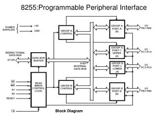
8255 PPI CHIP • One of the most widely used I/O chips. • It is a 40-pin DIP chip and has three separately accessible ports, A, B, and C, which can be programmed, hence the name PPI (programmable peripheral interface). • The individual ports can be programmed to be input or output. • They can also be changed dynamically, in contrast to the 74LS244 and 74LS373, which are hard-wired.
8255 PPI CHIP Port A (PA0 – PA7) (8-bit port) • Port A can be programmed all as input or all as output. Port B (PB0 – PB7) (8-bit port) • Port B can be programmed all as input or all as output. Port C (PC0 – PC7) (8-bit port) • Port C can be all input or all output. It can also be split into two parts, CU (upper bits PC4 - PC7) and CL (lower bits PC0 – PC3). Each can be used for input or output. Any of PC0 to PC7 can be programmed individually.
8255 PPI CHIP RD and WR • If the 8255 is using peripheral I/O design, IOR and lOW of the system bus are connected to these two pins. • If the port uses memory-mapped I/O, MEMR and MEMW activate them. RESET • This is an active-high signal input into the 8255 used to clear the control register. When RESET is activated, all ports are initialized as input ports. This pin must be connected to the RESET output of the system bus or ground, making it inactive. Like all IC input pins, it should not be left unconnected. This pin can be grounded.
8255 PPI CHIP A0, A1, and CS • While CS (chip select) selects the entire chip, address pins A0 and A1 select the specific port within the 8255. • These three pins are used to access ports A. B, C, or the control register, as shown in Table 11-3.
Mode selection of the 8255A While ports A, B, and C are used for I/O data, it is the control register that must be programmed to select the operation mode of the three ports A, B, and C. The ports of the 8255 can be programmed in any of the following modes. 1. Mode 0, simple I/O mode. In this mode, any of the ports A, B, CL, and CU can be programmed as input or output. In this mode, all bits are out or all are in. In other words, there is no control of individual bits. Mode 0 is the most widely used mode in current system I/O interfacing design. 2. Mode 1. In this mode, ports A and B can be used as input or output ports with handshaking capabilities. This mode is not used due to timing incompatibility with devices such as the printer. 3. Mode 2. In this mode, port A can be used as a bidirectional I/O port with handshaking capabilities. This mode is rarely used.
Notice from Figure 11-12 that we must set D7 = 1 to get the above I/O modes of 0,1, and 2. If D7 = 0, we have BSR mode. In BSR (bit set/reset) mode, the bits of port C are programmed individually. This mode is also rarely used.
The 8255 chip is programmed in any of the modes (Mode 0, 1 or 2) by sending a byte (or control word) to the control register of the 8255. For example to make ports A, B, and C input or output ports, we make D7 = 1 according to Figure 1112.
To select simple I/O mode of 0, we need 1000 0000 as the control word. • Similarly, to get PB as input, and PA and all of PC as output, we must have 1000 0010 or 82H for the control word.
Example 11-4: Find the control word if PA = out, PB = in, PC0- PC3 = in, and PC4 - PC7 = out.
Example 11-4: Find the control word if PA = out, PB = in, PC0- PC3 = in, and PC4 - PC7 = out. Solution: From Figure 11-12 we get the control word of 1000 0011 in binary or 83H 1 0 0 0 0 0 1 1 = 83H
Example 11-5: The 8255 shown in Figure 11-13 is configured as follows: port A as input, B as output, and all the bits of port C as output. (a) Find the port addresses assigned to A, B, C, and the control register. (b) Find the control byte (word) for this configuration.
(a) Find the port addresses assigned to A, B, C, and the control register. (a) The port addresses are as follows: (See Table 11-3) CSA1A0AddressPort 11000100 0 0 310H Port A 11000100 0 1 311H Port B 11000100 1 0 312H Port C 11000100 1 1 313H Control register
(b) Find the control byte (word) for this configuration. Port A as input, B as output, and all the bits of port C as output. Solution: (b) The control word is 90H, or 1001 0000. 1 0 0 1 0 0 0 0 = 90H