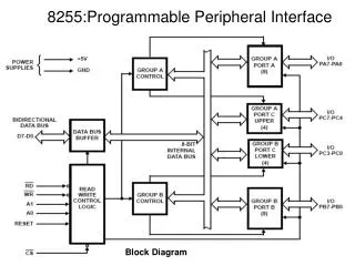
PROGRAMMABLE PERIPHERAL INTERFACE -8255
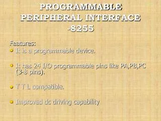
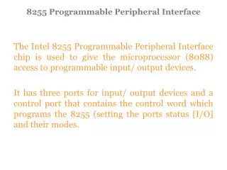
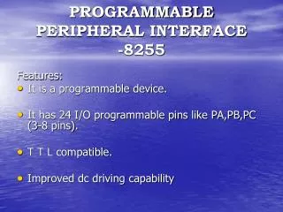
PROGRAMMABLE PERIPHERAL INTERFACE -8255. Features: It is a programmable device. It has 24 I/O programmable pins like PA,PB,PC (3-8 pins). T T L compatible. Improved dc driving capability . Pin Diagram. Function of pins:.

PROGRAMMABLE PERIPHERAL INTERFACE -8255
E N D
Presentation Transcript
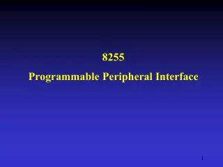
PROGRAMMABLE PERIPHERAL INTERFACE -8255 Features: • It is a programmable device. • It has 24 I/O programmable pins like PA,PB,PC (3-8 pins). • T T L compatible. • Improved dc driving capability
Function of pins: • Data bus(D0-D7):These are 8-bit bi-directional buses, connected to 8085 data bus for transferring data. • CS: This is Active Low signal. When it is low, then data is transfer from 8085. • Read: This is Active Low signal, when it is Low read operation will be start. • Write: This is Active Low signal, when it is Low Write operation will be start.
RESET: This is used to reset the device. That means clear control registers. • PA0-PA7:It is the 8-bit bi-directional I/O pins used to send the data to peripheral or or to receive the data from peripheral. • PB0-PB7:Similar to PA • PC0-PC7:This is also 8-bit bidirectional I/O pins. These lines are divided into two groups. • PC0 to PC3(Lower Groups) • PC4 to PC7 (Higher groups) These two groups working in separately using 4 data’s.
Data Bus buffer: • It is a 8-bit bidirectional Data bus. • Used to interface between 8255 data bus with system bus. • The internal data bus and Outer pins D0-D7 pins are connected in internally. • The direction of data buffer is decided by Read/Control Logic.
Read/Write Control Logic: • This is getting the input signals from control bus and Address bus • Control signal are RD and WR. • Address signals are A0,A1,and CS. • 8255 operation is enabled or disabled by CS.
Group A and Group B control: • Group A and B get the Control Signal from CPU and send the command to the individual control blocks. • Group A send the control signal to port A and Port C (Upper) PC7-PC4. • Group B send the control signal to port B and Port C (Lower) PC3-PC0. • PORT A: • This is a 8-bit buffered I/O latch. • It can be programmed by mode 0 , mode 1, mode 2 .
PORT B: • This is a 8-bit buffer I/O latch. • It can be programmed by mode 0 and mode 1. • PORT C: • This is a 8-bit Unlatched buffer Input and an Output latch. • It is splitted into two parts. • It can be programmed by bit set/reset operation.
Operation modes: BIT SET/RESET MODE: • The PORT C can be Set or Reset by sending OUT instruction to the CONTROL registers. I/O MODES: • MODE 0(Simple input / Output): • In this mode , port A, port B and port C is used as individually (Simply). • Features: • Outputs are latched , Inputs are buffered not latched. • Ports do not have Handshake or interrupt capability.
MODE 1 :(Input/output with Hand shake) • In this mode, input or output is transferred by hand shaking Signals. • Handshaking signals is used to transfer data between whose data transfer is not same. Computer Printer DATA BUS STB ACK Busy
Example: • The computer send the data to the printer large speed compared to the printer. • When computer send the data according to the printer speed at the time only, printer can accept. • If printer is not ready to accept the data then after sending the data bus , computer uses another handshaking signal to tell printer that valid data is available on the data bus. • Each port uses three lines from port C as handshake signals
MODE 2:bi-directional I/O data transfer: • This mode allows bidirectional data transfer over a single 8-bit data bus using handshake signals. • This feature is possible only Group A • Port A is working as 8-biy bidirectional. • PC3-PC7 is used for handshaking purpose. • The data is sent by CPU through this port , when the peripheral request it. • CONTROL WORD FORMATS: • In the INPUT mode , When RESET is High all 24 pins (3-ports) be a input mode.
i.e all flip flops are cleared and the interrupts are rest. • This condition is maintained even after RESET goes low. • This can be avoid by writing single control word to the control registers , when required.
FOR BIT SET/RESET MODE: • This is bit set/reset control word format. X X X Don’t care Bit select B0 B1 B2 BIT SET/RESET 1=SET 0=RESET BIT SET/RESET FLAG =0 Active
PC0-PC7 is set or reset as per the status of D0. • A BSR word is written for each bit • Example: • PC3 is Set then control register will be 0XXX0111. • PC4 is Reset then control register will be 0XXX01000. • X is a don’t care.
FOR I/O MODE: The mode format for I/O as shown in figure
The control word for both mode is same. • Bit D7 is used for specifying whether word loaded in to Bit set/reset mode or Mode definition word. • D7=1=Mode definition mode. • D7=0=Bit set/Reset mode.
Thank you Q&A