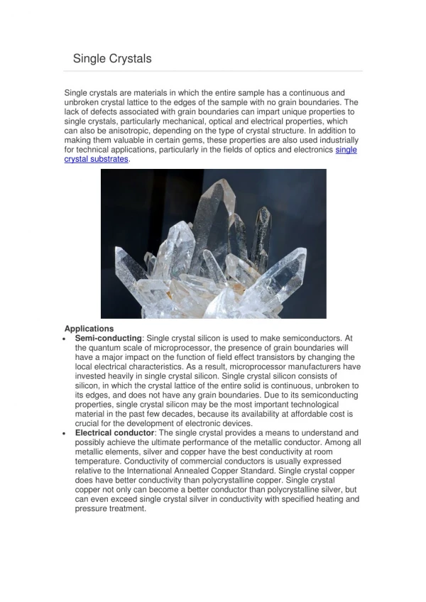
Download
1 / 14
140 likes | 307 Views
Effects of metallization on TlBr single crystals for detector applications. V. Kozlov a , M. Leskelä a , M. Vehkamäki a and H. Sipilä b. a Department of Chemistry, University of Helsinki, Finland b Oxford Instruments Analytical Oy, Espoo, Finland. TlBr properties.

E N D
Effects of metallization on TlBr single crystals for detector applications V. Kozlova, M. Leskeläa, M. Vehkamäkia and H. Sipiläb a Department of Chemistry, University of Helsinki, Finland b Oxford Instruments Analytical Oy, Espoo, Finland PSD-7, Liverpool, GB, 2005
TlBr properties • high atomic numbers Z: 81+35 => stopping power • density (7.56 g/cm3) => compact device • bandgap (2.68 eV) => room temperature • inter-pixel resistance ~500 GΩ (gap 100μm, 50V) => 2D-array detector* • optical transparency: 440nm – 50µm => scintillator? *Owens et al., Nucl. Instr. and Meth. A 531, 18 (2004) PSD-7, Liverpool, GB, 2005
Material problems • Purity • Crystal quality • Manufacturing process (Knoop hardness of 12 kg/mm2) • TlBr – toxic compound PSD-7, Liverpool, GB, 2005
Metallization methods Chemical: photographic process, Pd-dielectrics => possible water inclusion => X Glue: Ag- and graphite-paste => crater formation, if poor crystal quality properly treated samples: 2.5 kV/cm Physical: vapour (PVD), electron beam and sputtering deposition methods => Melt: metal melting on TlBr surface => PSD-7, Liverpool, GB, 2005
Interaction at the interface “Adhesion”: physical deposition “Diffusion” physical or melt methods “Compound” melt deposition or physical + annealing PSD-7, Liverpool, GB, 2005
Metal – Tl halide interface parameters TlBr (mp = 460oC) “Adhesion” “Diffusion” “Compound” Abr.: Atm. - unstable in atmosphere, Split. – Splitting X – Chemical reaction *Me-thickness – 0.5 μm units - MN/m2 [6, 8] PSD-7, Liverpool, GB, 2005
Results: Vacuum deposition Electron beam evaporation: thickness 25 and 40 nm Ti, Cr and Al • Ti and Cr: good electrical contacts, stable for ~year in a laboratory environment • Al: stable during all measurements for several days Fe and Ni – direct contact with TlBr molten => No reaction, if pure metals and complete degassing of system => Ni-boat was used for the melting of TlBr powder Output: - Ti, Cr, Fe and Ni elements were inert to TlBr - Ti and Cr could be used as reliable electrodes - Al ? PSD-7, Liverpool, GB, 2005
Results: Al/TlBr interface TlBr was deposed on a clean Al surface: (surface temperature control) • t < 100oC => fine films, R% spectra => stable for ~year, XRD • t > ~150oC => Tl-drops on Al => amorph. phase + Tl peaks Al(solid) + 3TlBr(gas) => 3Tl(drop) + AlBr3(gas) Output: no heating, low current PSD-7, Liverpool, GB, 2005
metal drop underlayer TlBr Results: Tl/, In/,Sn/TlBr interfaces Tl, In and Sn were shortly melted at ~310 oC: ( N2 atmosphere) • Sn: no reaction, no underlayer • In: Yellow underlayer compound ”pressed drop” on surface • Tl: Brown underlayer compound easily peeled off from TlBr + New process + annealing 20h => active reaction Output: Tl - aggressive with TlBr In PSD-7, Liverpool, GB, 2005
Results: In/,Sn/TlBr interfaces In and Sn were shortly melted at ~250 oC: (opposite side) • Sn, In: no reaction, no underlayer (In-case) • Sn: I-V characteristics of Sn-TlBr-Sn were asymmetrical for both electrodes => higher temperature for the intermediate compound Output: Sn electrode was reliable at our conditions. In TlBr In PSD-7, Liverpool, GB, 2005
Results: In/TlBr interface • In: I-V curves of In-TlBr-Layer-In => rectifier effect was observed (-) • High current connections: (+) Breakdown during further I-V & CV at ~200 V/cm Compare: working field 500 V/cm, Owens et al., Nucl. Instr. and Meth. A 531, 18 (2004) Output: low crystal quality, inner boundaries still limit the use of TlBr detector PSD-7, Liverpool, GB, 2005
Conclusions • Ti, Cr, Fe and Ni elements were inert to TlBr and Ti and Cr could be used as reliable electrodes. • Al contact can be used for tests at low current without heating. • Tl is reacting aggressively with TlBr. • Sn electrode was reliable at our conditions. • In was shown to form intermediate layer compound. • In/TlBr interface possesses rectifier properties; however, the crystal quality currently limits the use of this interface. PSD-7, Liverpool, GB, 2005
Acknowledgements • Crystal growth: I.S. Lisitsky and M. Kuznetsov (GIREDMET, Russia) • Finnish Technology Agency TEKES PSD-7, Liverpool, GB, 2005
END • Thank You! PSD-7, Liverpool, GB, 2005