CHAPTER 6 Virtex Memory
CHAPTER 6 Virtex Memory. Agenda. RAM Applications LUT RAM SRL 16 Other uses of LUT RAM (FIFO focus) Block RAM Inside Block RAM Cells. Operand stacks Register files Instruction caches DMA buffers Instruction memories State tables Logic functions Message buffers Virtual channels.

CHAPTER 6 Virtex Memory
E N D
Presentation Transcript
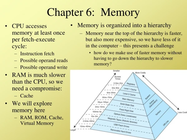
Agenda • RAM Applications • LUT RAM • SRL 16 • Other uses of LUT RAM (FIFO focus) • Block RAM • Inside Block RAM Cells
Operand stacks Register files Instruction caches DMA buffers Instruction memories State tables Logic functions Message buffers Virtual channels Video line buffers Digital delay lines RAMDAC color mapping tables Test vector buffers PCI configuration space Sequential machines More . . . RAM Applications
Linear Feedback Shift Regs. Galois style Fibonacci style
Virtex 5 32 X 2 Dual Port LUT RAM
Virtex 5 32 X 6 Dual Port LUT RAM
Asynchronous FIFO Issues • Problems with separate clock domains • Speed discrepancy between the two domains • Possibility of overflowing • Arrival rate/departure rate problem • Status communication • Glitching conditions on counters • Metastability • Would like nice, tidy “always works” solutions • Full details in Sunburst Design writeup by Cummings & Alfke
512 X 16 BRAM Module Comment: slide needs Inverter on one of the EN’s
Virtex 4 FIFO Support Structure (this stuff is inside the V4 BRAM module, built in)
8K X 4 Virtex 4 FIFO Cascading like this requires a 2 IN NOR be built in the LUT fabric
512 X 72 Virtex 4 FIFO Cascading like this needs 2 AND, 2 OR and 2 Inverters in LUT fabric
Virtex 5 Dual Port BRAM Symbol
Virtex 5 BRAM Organized X 64
Virtex RAM Closing Comments • RAM may be the primary on board feature beyond fabric of general use • Makes having other on board resources more effective • FIFOs –fast cross clock domain interfacing • Microprocessors – code/data storage • DSPs – on chip operand storage • And so on . . . • See XAPP 463 (appendix) for Verilog/VHDL code listing for using BRAM structure.