Download
1 / 10
100 likes | 215 Views
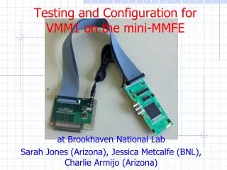
Testing and Configuration for VMM1 on the mini-MMFE. at Brookhaven National Lab Sarah Jones (Arizona), Jessica Metcalfe (BNL ), Charlie Armijo (Arizona). Testing the mini-MMFE. Adapter card, v1. TDO and PDO. FPGA. VMM1 ASIC. USB connection. Timing E xample for New S etup.

E N D
Testing and Configuration for VMM1 on the mini-MMFE at Brookhaven National Lab Sarah Jones (Arizona), Jessica Metcalfe (BNL), Charlie Armijo (Arizona)
Testing the mini-MMFE Adapter card, v1 TDO and PDO FPGA VMM1 ASIC USB connection
Timing Example for New Setup • At peak, ramp begins for timing between peak and readout signals. Slope of ramp gives conversion from voltage to time. Ideally, slope = constant
Noise Measurement Example • Noise measurements with RMS vs peaking time for various Gains (0.5, 1, 3, 9 mV/fC) • CHN 64 noise:
Plans • Testing of the mini-MMFE was successful with only minor issues • Next steps are to: • Assemble remaining 10 mini-MMFE (left-handed) this week and begin testing at BNL late next week • Fabricate V2 adapter card (with LVDS to RSDS conversions) this week • May not be needed but will have it anyway • Begin layout of right-handed mini-MMFE • Few day job
Issues with Current Boards • Digital ground and digital signal switched • ena and wen signal pins switched • a0-a5 address pins switched in order • TDO and PDO signal connectors switched • Ribbon cables (for 60 to 60 pin) are difficult to construct • Silkscreen issues
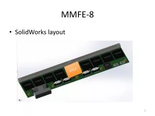
New “C-Card” Existing BNL DAQ board with ADCs and Cyclone IV for readout, configuration • AZ Adapter Card (V1) AVNET LX9 with Spartan 6 FPGA for ethernet connection to switch
DAQ Status and Plans • UDP datagram sent between client and server at Arizona • Can be used for testing with Mamma DAQ • UDP datagram sent from LX9 at Harvard • Will be tested at Arizona this week • Communication between Jack’s BNL DAQ board and LX9 progressing well • Integration at BNL 7/2 – 7/11 including George Iakovidis et al. • Need meeting with Marcin on Mamma DAQ end
UDP Server UDP Client UDP Datagram ACK • UDP client and server are running on a LAN. • We have sent a big-endian datagram via the UDP client on the laptop, which is a sample event in the current format. • We have received the datagram on a desktop computer and unpacked three 32-bit words of the event to correctly obtain each address, timing, and amplitude included. • The server sends an ack, which in this case completes the transaction. • The Spartan6 LX9 will replace the laptop as soon as we get the compiled image.