MMFE-8
MMFE-8. SolidWorks layout. FPGA. MMFE-8 PCB. Local OSC. Config Flash. Config JTAG. MMFE_8 w/ FPGA Block Diagram. SPI MOSI to VMM2_1 CONFIG + CLK. 10. Artix XC7A200T-2FBG676Cv. 8. SPI MISO from VMM2. TTC, CTRL, Status Clk. 74. 4. L1 Sync, L1 Clk. ADC. 24. 2. ART Clk.

MMFE-8
E N D
Presentation Transcript
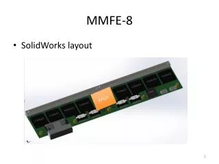
MMFE-8 • SolidWorks layout FPGA
Local OSC Config Flash Config JTAG MMFE_8 w/ FPGA Block Diagram SPI MOSI to VMM2_1 CONFIG + CLK 10 ArtixXC7A200T-2FBG676Cv 8 SPI MISO from VMM2 TTC, CTRL, Status Clk 74 4 L1 Sync, L1 Clk ADC 24 2 ART Clk BCnt + Ctrl SPI CFG ACLK L1 Accept TRIG/ADDR: 16 2 64 Sig In Dual Zebra + Protection VMM2_1 6 BCnt + Ctrl SPI CFG ACLK L1 Accept D0, D1, STATUS: 48 2 64 Sig In VMM2_2 6 BCnt + Ctrl SPI CFG ACLK L1 Accept Protection 2 uHDMI SRS 64 Sig In VMM2_3 6 BCnt + Ctrl SPI CFG ACLK L1 Accept 2 64 Sig In GbE PHY uHDMI GbE VMM2_4 6 BCnt + Ctrl SPI CFG ACLK L1 Accept 2 64 Sig In VMM2_5 uHDMI GBT 6 BCnt + Ctrl SPI CFG ACLK L1 Accept 2 64 Sig In VMM2_6 6 BCnt + Ctrl SPI CFG ACLK L1 Accept miniSAS 8i 2 64 Sig In VMM2_7 6 BCnt + Ctrl SPI CFG ACLK L1 Accept 2 64 Sig In VMM2_8 6 VMM 1.2 VDC_Analog VMM 1.2 VDC_Digital FPGA 1.8/1.2/1.0 VDC 24 VDC
MMFE-8 • Input • 2 x 256 channel Zebra connectors (Ruter Elastomer) • Compatible with sTGC • 24V Power connector TBD • Input / Output • JTAG for FPGA Configuration • ≤ 68pin miniSAS 8i I/O (e-link) • μHDMI for SRS (still TBD with Sorin) • μHDMIfor future dual GBT or dual e-link • μHDMIfor ethernet
I/O Connections between FPGA and VMMs • Configuration (3 pairs) • Configuration clock (potential multidrop) • di and d0 • ART Data (2 pairs) • ART clock (potential multidrop) • ART data to ART ASIC • L1 Data (4 pairs) • L1 Data clock (potential multidrop) • SYNCH • L1 Data (d0 and d1) • TTC (5 pairs) • BC clock (phase adjusted) (potential multidrop) • L1A (potential multidrop) • BCR (potential multidrop) • FER (potential multidrop) • CAL • Control (2 pairs) • WEN and ENA • Status (2 pairs) • VMM status • Status clock (potential multidrop) Implies Worst Case 18 x 8 = 144 pairs (288 pins) for FPGA Implies Best Case 10 x 8 + 8 - 8 = 88 pairs (160 pins) for FPGA (pairs + MD – ART)
Connections between FPGA and MMFE-8 I/O • SRS uHDMI(need Sorin’sinput) (4 pairs) • 4 undefined pairs • GbEuHDMI(4 pairs) • 4 pairs from PHY (need magnetics and adapter) • 14 pins to PHY from FPGA • GTB uHDMI (3 pairs) • 2, 3, or 4 pairs depending on application (single, dual, GTB or e-link) • miniSAS 8i (24 pairs) • Configuration, Control and Status (3 pair e-link) • Configuration (encoded) • WEN and ENA (encoded) • Status (encoded) • TTC (3 pair e-link) • BC clock (phase adjusted e-link clk) • L1A (encoded) • BCR (encoded) • FER (encoded) • CAL (encoded) • JTAG (encoded) • L1 Data (3 pair e-link) • ART data (8 + 1 =9 pairs) • JTAG(4 pins) • sTGC needs? TTP signals are currently left open… Implies 36pairs (72pins) For FPGA Implies 18 pairs (36 pins) For miniSAS 8i
FPGA Choice • Design files exist for S6 and K7 (Arizona) and A7 (Weizmann) • Vivado can be used with *7 FPGA’s • Zynq has ARM capability (easier testing via C?) • S6 needs fewer voltages • A7, K7, Z7 have ADC capabilities • Chose XC7A200T-2FBG676C • Best known architecture and tools • 3 rail power solution • No bank restrictions • Has MB solution available • Nearly identical dev board and IP • Good chance of Rad Hard acceptance • Comparable cost $250 • Comparable size 729mm • Comparable power ~600mW quiescent
FPGA Power Estimate • Xilinx Power Management Solutions Guide from Analog Devices • 1V -- ICCINT=3.15A; ICCBRAM=.100A?; IMGT_AVCC=.511A =>3.66A • 1.2V -- ICCIO=0.1A; IMGT_AVTT=0.36A; ICCO=.511A => .971A • 1.8V – ICCAUX=0.32A • Next: XPE Power Estimation—Use Cases for Artix-7/Kintex-7
VMM Power Estimate • VMM requires separate Analog 1.2V supply, 8mW/ch * 64 = 512mW => 427mA. • VMM requires separate Digital 1.2V supply, 10mW/pr* 18 = 180mW => 150mA. • 8 VMM’s require Ivmma = 3.4A; Ivmmd = 1.2A
Power Solution • 1 x LTM4619 • Drop 24Vin to 1.8Va for Vvmma • Drop 24Vin to 1.8Vd for Vvmmd • Use 1.8Vd for 1.8Vfpga • 2 x 8 LT3080 • Drop 1.8Va to 1.2Va for Vvmma • Drop 1.8Vd to 1.2Vd for Vvmmd • Awaiting Gianluigi’s feedback • 1 x LTM4619 • Drop 24Vin to 1.2Vfpga • Drop 24Vin to 1.0Vfpga • Utilize additional LTM4619 if required. • LTM4619 and LT3080 have successful Rad Hard history. • Use Chip Inductors liberally to separate power inputs, permit direct current measurement. • Use Bulk and Bypass Caps Liberally to reduce supply noise.
Analog Input Considerations:Protection: • NUP4114 is the current protection device in use. • ESD Rating for contact is +/- 8 KV • Capacitance is 1 - 0.3pf • New proposed ESD7008 has: • Same manufacturer • Lower capacitance 0.2pf • Higher ESD Rating for contact +/- 15 KV • Comparable cost per channel • Slightly larger packaging (to dissipate energy) • Bidirectional capability • Testing leakage current now…
Analog / Digital Design Considerations • Analog Power should not overlap Digital ground planes, and vice versa. • Analog length matching is not important, however impedance matching is. • Digital length and impedance matching is important, within pairs, and within clock domains. • Distributed clocks such as ART to VMM should be the same distance from the FPGA.
Configuration • Startup FPGA configuration should be stored in the config flash, This will speed up startup. • A Golden config should be kept in flash, to speed recovery. • VMM config should be stored in flash. • Flash can be configured via JTAG. • A serial number can be stored in the flash.
ADC • ADC is built into the FPGA. • 32 Channels • 12bit • 1MHz • 0-1V • 3 ADC lines can be provided to each VMM from the FPGA, for cal and diagnostics. • ADC also monitors Power and Temp.
Readout of MMFE-8 The Spartan 6 on the S6-FMC is used to translate voltage levels to/from VMM Custom S6-FMC GbE out (UDP packets) Or Versa- Link (Custom packets) 4 x miniSAS cables (32 ART, 3+ E-Link each) GbE out (UDP packets) to MATLAB 4 x MMFE-8, each containing 8VMM ASICs The Virtex 6 contains transfer logic to configure and readout the VMM PCIeout packets to Chassis
Readout of MMFE-8 The Spartan 6 on the S6-FMC is used to translate voltage levels to/from VMM GbE out (UDP packets) Or Versa- Link (Custom packets) 4 x miniSAS cables (32 ART, 3+ E-Link each) GbE out (UDP packets) to MATLAB 4 x MMFE-8, each containing 8VMM ASICs The Virtex 6 contains transfer logic to configure and readout the VMM PCIeout packets to Chassis