JEM Update: Progress on Hardware, Firmware, and Upcoming Tests
This summary captures the current status and advancements in the JEM project, detailing the redesign and operational tests of JEM modules. JEM0.0 has been successfully used for standalone tests, while JEM0.1 is fully qualified and JEM0.2 is in production. The firmware is extensively tested, with remaining tasks focusing on input synchronization and FIO link tests. Planned upgrades address PCB design challenges, with a shift to enhanced signal integrity components. Key testing phases and the need for final adjustments before transitioning to production are highlighted.

JEM Update: Progress on Hardware, Firmware, and Upcoming Tests
E N D
Presentation Transcript
JEM Plans • Status (summary) • Further standalone tests • Sub-slice test programme • JEM re-design • Slice test
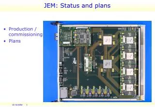
Status (summary) • 2 JEMs up and running: JEM0.0 used for standalone tests only JEM0.1 fully qualified module0 • 1 JEM under production: JEM0.2 (=JEM0.1 with larger main processor (XCV1600E) • Hardware fully tested, apart from CAN and flash configurator. Systematic tests of FIO links soon. • Firmware fully tested apart from final input synchronisation, final jet code and ROI • Work on merger RTDP starting now • Control software available. Final software (module services and HDMC) under way • JEM0 documentation has been updated V.8g
Further standalone tests A few further tests are required before moving to RAL: • Final input synchronisation • FIO link tests with adjustable TTC clock • final level2 interface (ROI)
JEM0.1/0.2 Sub-slice test at RAL Ready for tests at RAL this month Hardware required : • powered crate w. backplane and TCM etc. • 1-2 JEM0s w. TTC daughters • LVDS signal sources • Access to TTC-system for non-exclusive use • Merger, ROD (+6U-crate, CPU, 1 DSS, on-line software … shipped from Mainz) Test: • Large numbers of input channels (DSSs) • Timing with (real) TTC • Inter-JEM communication on Processor Backplane • Merger communication (energy merger w. simplified RTDP ?) • Slice data into RODs ( ?? or any other sink ?)
Towards the production modules:Why a new JEM design? (what‘s wrong with the old one) • Current JEM is 1.6mm PCB. Cannot be turned into 2mm due to component height on bottom of PCB final JEP would require special crate with 1.6mm rails in JEM slots • A large fraction of signal lines are currently not JTAG B/scannable due to old LVDS devices • Current main processor is expensive and slow (XCV1600E-6 : 1500 €) • Main processor would benefit from XC2V hardware multipliers (latency) • Virtex-2 input processors could improve signal integrity on FIO • TTC circuitry needs to be revised. (use fBGA, attach to ROC rather than control FPGA) • Minor revisions on incoming links (no jumpers for chassis GND) • Minor revisions of clock distribution • VME access needs to be revised (long unbuffered address lines) • Flash ROM configuration scheme needs to be revised • Final CAN interface
JEM Re-design (baseline) • Main processor: XC2V2000 (hardware multipliers) • B/Scan-able de-serialisers : 6-channel device SCAN921260 • Compatible to DS92LV1021/3 series • 196-pin, 1mm BGA package • Input Processors 4*XC2V1500 • ROC/TTC interface XC2V1500 • Board control (VME etc.) XC2V500 • TTCrx chip on JEM • Bring DCS and TTCrx access(VME) in line with CPM design. Re-targeting VHDL code to Virtex2 will require some ( minor ) work on instantiated components: DLLDCM, 4kbit RAM 18kbit RAM
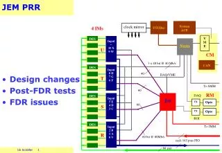
JEM 15 x 6-channel de-serialisers : SCAN921260 4 Input Processors : XC2V1500 Main Processor XC2V2000 6 links per de-serialiser DCS Input Processor Config VME VME Input Processor Main Processor Input Processor 6 ROC TTC G Input Processor G 15* '921260 88 LVDS links
PCB design issues • De-serialisers, TTCrx and XC2V are fBGAs with virtually no unused pins. 3 supply voltages (digital, analog, PLL) on de-serialisers. • High density of vias VCC/GND planes perforated need small vias, low clearances from via to GND/VCC high accuracy required • Huge PCB • PCB thickness increased to 2mm (compatibility) • Small via diameters not possible with thick PCBs • We need high VCC/GND distributed capacitance thin FR4 sheets/prepreg (shrinkage) reduced accuracy
JEM1 Due to PCB issues, work on schematics has been discontinued and layout of a sub-set of the schematics was started: Preliminary layout of input block with 4 de-serialisers and one input FPGA is under way and is being discussed with the PCB manufacturer (Andus). • cost, technology (blind vias, micro vias,..?), timescale Fallback solution: old-style JEM 1.6mm, daughter boards ? Even though there won‘t be large amounts of (ATLAS) money spent on the first batch of JEM1s, a review will be appropriate due to technological challenges.
JEM1 First feedback from PCB manufacturer: • We share our problems with everyone using modern fBGA devices with full ball array as opposed to ring of balls. • Urged to go to 1.6mm PCB. It is no problem to have thicker board edges that fit the rails. Mechanical structures within a PCB are standard technology. Even integrated stiffeners are possible, if required. • With 1.6mm thickness 250 µm vias are possible. We are guaranteed to have 150µm of metal between two 1mm spaced vias. Recommendation for power planes: use GND/VCC/GND sandwiches throughout to increase distributed capacitance.
Full slice test Slice test will take place in x/2003 • JEM0.1 is available now • JEM0.2 is under production now • 1-2 JEM(s)0 will be submitted in (x-2.5)/2003 • Have JEMs1.0 available in ongoing slice test at a later stage • JEM1 seriously different from JEM0, expect minor PCB revisions (JEM1.1) for production modules