Efficient Configuration and Flash Updates for JEM FPGA Modules via VME and SystemACE
This guide outlines the process for configuring and updating the firmware of JEM FPGA modules, employing SystemACE for CompactFlash loading. FPGAs require a configuration file post-power-up to define their functionality, typically sourced from external flash memory. Steps include generating a configuration file with IMPACT, utilizing a USB flash adapter to write it to a CF card, and updating the flash via VME connections. Recent firmware improvements address glitches in data strobes, enhancing reliability and enabling successful updates without entering the pit.

Efficient Configuration and Flash Updates for JEM FPGA Modules via VME and SystemACE
E N D
Presentation Transcript
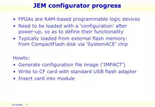
JEM configurator progress • FPGAs are RAM-based programmable logic devices • Need to be loaded with a ‘configuration’ after power-up, so as to define their functionality • Typically loaded from external flash memory: from CompactFlash disk via ‘SystemACE’ chip Howto: • Generate configuration file image (‘IMPACT’) • Write to CF card with standard USB flash adapter • Insert card into module
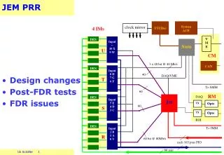
JEM block diagram CFcard System ACE clock mirror DES V M E Input -- 10 X 9 W Sum Configuration: 6 FPGAs SystemACE chip CF card VME interface built from programmable logic (CPLD = non-volatile device) ---------------------- SystemAce physically connected to VME Should be possible to flash the cards while in the module TTCdec U To SMM 3 x 40 bit @ 40 Mb/s DES Input 8 H 7 G 6 F DAQ 40 DAQ/Timing/VME T Opto G Opto G 60 ROI DES Jet Input 5 E 4 D 3 C 60 S CAN DES To JMM Input 2 B 1 A 0 V R 60 bit @ 80Mb/s each 165 pins FIO 88 pair
In-situ flash update via VME • Connect SystemACE to VMEbus via CPLD (firmware) • Have crate CPU write the flash image from file through SystemACE chip onto CF disk • Create empty disk image file • Loop-mount on any Linux computer • Copy configuration files into image • Umount and transfer to target system • Have custom software write image to CompactFlash disk • Status by Summer 2008: • Flash writer works in Mainz • Fails at CERN (USA15) for unknown reason give up • March / April, 2009: Richard Staley (B’ham) discovers and explores an issue with the L1Calo VME subsystem:VME mount module (VMM) generates data strobes not compliant with VME specs
VME issue • Date strobe exhibits glitches • For write operations these glitches trigger read operations after a valid write access on B’ham modules • No problems seen so far on JEMs, except... DS0* WRITE*
Refurbish flash write firmware • Keep flasher software nearly unchanged • Re-work firmware such that read access is protected from glitches • Start read operations only if data strobe asserted for a minimum of 50ns • Finish internal read operations after a predefined delay, do not wait for data strobe being deasserted • Latch the data until VME cycle finished Results: • Test rig Mainz : new firmware ok now, though 2008 version fails ! • Test week June 15: • Flash card writer error-free on CERN test rig • Error-free in USA15, all 32 JEM modules could be updated after a somewhat lengthy CPLD update procedure (successful thanks to Andrea)
What next... • No more need to enter the pit for FPGA firmware updates • VME access tightened for flash card operations only, since no problems had been observed elsewhere • Keep an eye on reliability of VME operations and have further refurbishment in case instabilities are observed Unfortunately, for any update of the VME CPLD we would again have to enter USA15 and reload each JEM individually. That would be a major intervention, if required during ATLAS running...