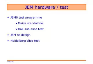
JEM hardware / test
JEM hardware / test. JEM0 test programme Mainz standalone RAL sub-slice test JEM re-design Heidelberg slice test. Redesign: current JEM0.1 module. 88 de-serialisers : DS92LV1224 11 Input Processors : XC2S200 Main Processor XCV600E/1000E. Input proc. JEM0.0 -top view-. terminator. 20.

JEM hardware / test
E N D
Presentation Transcript
JEM hardware / test • JEM0 test programme • Mainz standalone • RAL sub-slice test • JEM re-design • Heidelberg slice test
Redesign: current JEM0.1 module 88 de-serialisers : DS92LV1224 11 Input Processors : XC2S200 Main Processor XCV600E/1000E
Input proc. JEM0.0-top view- terminator 20 15 15 Main Deser.
Standalone tests at Mainz, JEM0.1 • VME: no dedicated tests, VME used to test all other aspects of JEM functionality. • Timing: No TTC available at Mainz (TTCvi missing). No expertise nor resources available to set up a system in Mainz. Currently using 40MHz clock from DSS. • Real-time D.P. (sum): 88 de-serialisers to be fed by link replicator module via twist’n flat cable. Results spy memory VME. Test vectors: Thomas (Gilles). Backplane signals to be checked with oscilloscope. • RTDP (jet): Need help from Stockholm. For data integrity inter-JEM communication requires programmable clock in main processor. This is available from the TTCrx only. Standalone tests w. external delay unit and micro-backplane feeding the FIO lines back to the same JEM ? • DAQ&ROI: No test hardware available. Data could be sunk into DSS, if required (ROC firmware to be completed first!). • Configurator: currently FPGA configuration via VME only. No further work will be done on configuration hardware. On future JEMs use CP-compatible configurator hardware. No tests at Mainz. • CAN: no compatible hardware on the final modules no effort to complete and test the ELMB-based DCS interface.
JEM0.1 Sub-slice test at RAL (MZ and Stockholm) Start tests at RAL in autumn after first successful CPM tests • Timing with TTC • Inter-JEM communication on PB • Merger communication • Slice data into RODs Hardware required (in this order…) : • powered crate w. backplane • 2 JEM0s w. TTC daughter • Access to TTC-system for non-exclusive use • Sum & jet merger • ROD(s) (+6U-crate, CPUs, 1 DSS, on-line software … shipped from Mainz)
Redesign : JEM0.9 (capture starts 8/2002) • Need to turn main processor into Virtex2 (hardware multipliers) • B/Scan-able deserialisers : 6-channel device SCAN921260 • Compatible to DS92LV1021/3 series (same core ?) • 196-pin, 1mm BGA package • Need to increase logic resources on Input Processors (see next slide) • Try to use only one FPGA family on JEM Virtex2(cost !) • Turn on-board VME to proper VME--, if device pin count allows • Finalise TTC circuitry • Bring DCS, FPGA configurator, and TTCrx access(VME) in line with CPM design. Try to provide enough resources to also unify DAQ/ROI code at a later stage. Re-targeting VHDL code to Virtex2 will require some ( minor ) work on instantiated components: DLLDCM, 4kbit RAM 18kbit RAM
Input Processors On JEM0.1: XC2S200-7FG456C too small Upgrade to: • XC2S300E-6FG456C @ $67 (costing) cheap • XCV300E-6FG456C @ $160 • XC2V500E-4FG456C @ $160 • 1/3 of XC2V1500E-4FF896C @ $525/3! 520€ incl. VAT All devices have similar logic resources, XC2S300 is low in block memory resources, no further upgrade available in Spartan family. Speed grades are equivalent. All pricing Avnet.com base price. Virtex2 will allow to drop terminator resistors (DCI)
FPGAs on JEM0.9 Pin budget (real-time data path only): • Main processor (80Mb/s in+merger out) 385+50 =435 • Input processor (des. in + 80Mb/s out) 24*12+3*35 =393 + clocks + VME + ROC + configuration pins… XC2V1500-FF896 has 528 user I/O For the main processor an upgrade to XC2V2000 (624 user I/O) might be considered (decide soon).
JEM0.9 15 x 6-channel de-serialisers : SCAN921260 4 Input Processors : XC2V1500 Main Processor XC2V1500/2000 Final partitioning of serialisation into FPGA devices to be discussed Compatibility of control circuitry to CP ! VME 6 links per de-serialiser Input Processor config timing DCS Input Processor Main Processor Input Processor 6 G ROC Input Processor G 15* '921260 88 LVDS links
Slice test at HD In early 2003 JEM0.9 should be available. It is assumed to be B/Scan-able to a large extent and firmware compatible to JEM0.1, as far as RTDP, DAQ&ROI, playback & spy are concerned move to HD after quick standalone tests (assuming ongoing tests on JEM0.1 do not reveal problems at a late stage). • Repeat previous sub-slice tests • Run ROI tests with 3 or 4 modules • Test all circuitry not available on JEM0.1 in full slice.