Download
1 / 61
610 likes | 771 Views
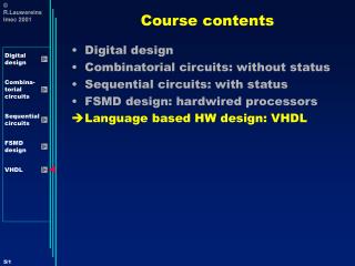
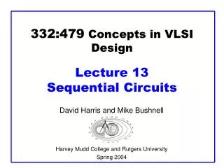
332:479 Concepts in VLSI Design Lecture 13 Sequential Circuits. David Harris and Mike Bushnell Harvey Mudd College and Rutgers University Spring 2004. Outline. Floorplanning Sequencing Sequencing Element Design Max and Min-Delay Clock Skew Two-Phase Clocking Summary.

E N D
332:479 Concepts in VLSIDesignLecture 13 Sequential Circuits David Harris and Mike Bushnell Harvey Mudd College and Rutgers University Spring 2004
Outline • Floorplanning • Sequencing • Sequencing Element Design • Max and Min-Delay • Clock Skew • Two-Phase Clocking • Summary Material from: CMOS VLSI Design By Neil E. Weste and David Harris Concepts in VLSI Des. Lec. 13
Project Strategy • Proposal • Specifies inputs, outputs, relation between them • Floorplan • Begins with block diagram • Annotate dimensions and location of each block • Requires detailed paper design • Schematic • Make paper design simulate correctly • Layout • Physical design, DRC, NCC, ERC Concepts in VLSI Des. Lec. 13
Floorplan • How do you estimate block areas? • Begin with block diagram • Each block has • Inputs • Outputs • Function (draw schematic) • Type: array, datapath, random logic • Estimation depends on type of logic Concepts in VLSI Des. Lec. 13
MIPS Floorplan Concepts in VLSI Des. Lec. 13
Area Estimation • Arrays: • Layout basic cell • Calculate core area from # of cells • Allow area for decoders, column circuitry • Datapaths • Sketch slice plan • Count area of cells from cell library • Ensure wiring is possible • Random logic • Compare complexity do a design you have done Concepts in VLSI Des. Lec. 13
MIPS Slice Plan Concepts in VLSI Des. Lec. 13
Typical Layout Densities • Typical numbers of high-quality layout • Derate by 2 for class projects to allow routing and some sloppy layout. • Allocate space for big wiring channels Concepts in VLSI Des. Lec. 13
Sequencing • Combinational logic (CL) • output depends on current inputs • Sequential logic • output depends on current and previous inputs • Requires separating previous, current, future • Called state or tokens • Ex: FSM, pipeline Concepts in VLSI Des. Lec. 13
Pipelined System • Huffman Model Finite State Machine (FSM) & pipelined system Concepts in VLSI Des. Lec. 13
Sequencing (cont’d.) • If tokens moved through pipeline at constant speed, no sequencing elements would be necessary • Ex: fiber-optic cable • Light pulses (tokens) are sent down cable • Next pulse sent before first reaches end of cable • No need for hardware to separate pulses • But dispersion sets min. time between pulses • This is called wave pipelining in circuits • In most circuits, dispersion is high • Delay fast tokens so they don’t catch slow ones. Concepts in VLSI Des. Lec. 13
Sequencing Overhead • Use flip-flops to delay fast tokens so they move through exactly one stage each cycle. • Inevitably adds some delay to the slow tokens • Makes circuit slower than just the logic delay • Called sequencing overhead • Some people call this clocking overhead • But it applies to asynchronous circuits too • Inevitable side effect of maintaining sequence Concepts in VLSI Des. Lec. 13
Sequencing Elements • Latch: Level sensitive • a.k.a. transparent latch, D latch • Flip-flop: edge triggered • A.k.a. master-slave flip-flop, D flip-flop, D register • Timing Diagrams • Transparent • Opaque • Edge-trigger Concepts in VLSI Des. Lec. 13
Sequencing Elements • Latch: Level sensitive • a.k.a. transparent latch, D latch • Flip-flop: edge triggered • A.k.a. master-slave flip-flop, D flip-flop, D register • Timing Diagrams • Transparent • Opaque • Edge-trigger Concepts in VLSI Des. Lec. 13
Latch Design • Pass Transistor Latch • Pros + + • Cons Concepts in VLSI Des. Lec. 13
Latch Design • Pass Transistor Latch • Pros + Tiny + Low clock load • Cons • Vt drop • nonrestoring • backdriving • output noise sensitivity • dynamic • diffusion input Used in 1970’s Concepts in VLSI Des. Lec. 13
Latch Design • Transmission gate + - Concepts in VLSI Des. Lec. 13
Latch Design • Transmission gate + No Vt drop - Requires inverted clock Concepts in VLSI Des. Lec. 13
Latch Design • Inverting buffer + + + Fixes either Concepts in VLSI Des. Lec. 13
Latch Design • Inverting buffer + Restoring + No backdriving + Fixes either • Output noise sensitivity • Or diffusion input • Inverted output Concepts in VLSI Des. Lec. 13
Latch Design • Tristate feedback + Concepts in VLSI Des. Lec. 13
Latch Design • Tristate feedback + Static • Backdriving risk • Static latches are now essential Concepts in VLSI Des. Lec. 13
Latch Design • Buffered input + + Concepts in VLSI Des. Lec. 13
Latch Design • Buffered input + Fixes diffusion input + Noninverting Concepts in VLSI Des. Lec. 13
Latch Design • Buffered output + Concepts in VLSI Des. Lec. 13
Latch Design • Buffered output + No backdriving • Widely used in standard cells + Very robust (most important) • Rather large • Rather slow (1.5 – 2 FO4 delays) • High clock loading Concepts in VLSI Des. Lec. 13
Latch Design • Datapath latch + - Concepts in VLSI Des. Lec. 13
Latch Design • Datapath latch + Smaller, faster - Unbuffered input Concepts in VLSI Des. Lec. 13
Flip-Flop Design • Flip-flop is built as pair of back-to-back latches Concepts in VLSI Des. Lec. 13
Enable • Enable: ignore clock when en = 0 • Mux: increase latch D-Q delay • Clock Gating: increase en setup time, skew Concepts in VLSI Des. Lec. 13
Reset • Force output low when reset asserted • Synchronous vs. asynchronous Concepts in VLSI Des. Lec. 13
Set / Reset • Set forces output high when enabled • Flip-flop with asynchronous set and reset Concepts in VLSI Des. Lec. 13
Positive Edge Triggering Concepts in VLSI Des. Lec. 13
Negative and Positive Latches Concepts in VLSI Des. Lec. 13
Positive Edge-Triggered Reg. Concepts in VLSI Des. Lec. 13
T Flip-Flop Concepts in VLSI Des. Lec. 13
JK Flip-FLop Concepts in VLSI Des. Lec. 13
Sequencing Methods • Flip-flops • 2-Phase Latches • Pulsed Latches Concepts in VLSI Des. Lec. 13
Timing Diagrams Contamination and Propagation Delays Concepts in VLSI Des. Lec. 13
Max-Delay: Flip-Flops Concepts in VLSI Des. Lec. 13
Max-Delay: Flip-Flops Concepts in VLSI Des. Lec. 13
Max Delay: 2-Phase Latches Concepts in VLSI Des. Lec. 13
Max Delay: 2-Phase Latches Concepts in VLSI Des. Lec. 13
Max Delay: Pulsed Latches Concepts in VLSI Des. Lec. 13
Max Delay: Pulsed Latches Concepts in VLSI Des. Lec. 13
Min-Delay: Flip-Flops Concepts in VLSI Des. Lec. 13
Min-Delay: Flip-Flops Concepts in VLSI Des. Lec. 13
Min-Delay: 2-Phase Latches Hold time reduced by nonoverlap Paradox: hold applies twice each cycle, vs. only once for flops. But a flop is made of two latches! Concepts in VLSI Des. Lec. 13
Min-Delay: 2-Phase Latches Hold time reduced by nonoverlap Paradox: hold applies twice each cycle, vs. only once for flops. But a flop is made of two latches! Concepts in VLSI Des. Lec. 13
Min-Delay: Pulsed Latches Hold time increased by pulse width Concepts in VLSI Des. Lec. 13