Download
1 / 17
180 likes | 377 Views
Improvement in scintillation counter energy resolution with the silicon drift detector. *Shuji Maeo 1,2 , Takayuki Yanagida 1 , Yuui Yokota 1 and Akira Yoshikawa 1,3.

E N D
Improvement in scintillation counterenergyresolution with the silicondrift detector *Shuji Maeo1,2, Takayuki Yanagida1, Yuui Yokota1 and Akira Yoshikawa1,3 1Division of Physical Process Design,Institute of Multidisciplinary Research for Advanced Materials (IMRAM),Tohoku University 2Japan Association for the Advancement of Medical Equipment 3New Industry Creation Hatchery Center(NICHe), Tohoku University
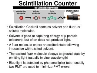
Introduction • High energy radiation measurements • Scintillation counter is useful. Radiation Light Electrical signal To processor… Scintillator Light detector Typical detector is Photo Multiplier Tube(PMT). Problems Energy resolution is not enough. It can not use in magnetic fields. ・In Conventional photo diode(PD), signal intensity is low, noise level is high(low S/N ratio). ・In Avalanche PD(APD), S/N ratio is not so high. Going to semiconductor
Scope of research • Improvement of S/N ratio in Scintillation counter • Using an Silicon drift detector(SDD) as light detector High energy resolution ↓ Applying PD array etc. ↓ High contrast imaging In this report • Estimations using the SDD • Problems and Next plan
Electron can be collected efficiently for electric field formed by ring like cathode. • Anode capacitance is low for small anode size.. • Field Effect Transistor(FET) can be constructed at SDD directly. • Thermal noise can be reduced for cooling by the peltier cooler. • High energy resolution and high count rate are available. Characteristics of the SDD Structure of the SDD P. Lechner et al., Nucl. Instrum. Methods, vol. A-377,346 (1996).
Affects of energy resolution Simulation results of peak shape depended on each resolution.
Comparison of X-ray response Np-Lα 13.9keV Np-Lβ 17.7keV Np-Lβ 17.7keV FWHM:1.7keV (2.9%) FWHM:0.8keV (1.3%) Np-Lα 13.9keV Np-Lγ 20.8keV Np-Lγ 20.8keV γ 59.5keV γ 26.4keV γ 59.5keV γ 26.4keV Spectrum of 241Am measured by conventional Si-pinPD Spectrum of 241Am measured by the SDD Hamamatsu (S1722-02) KETEK
Linearity of the pulse heightfor X-rays Np-Lβ 17.7keV Np-Lα 13.9keV Np-Lγ 20.8keV γ 59.5keV γ 26.4keV Calibration curve It can be estimated that linearity between pulse height and energy.
Linearity of the pulse heightfor visible light Red LED voltage / mV 100 200 300 400 500 600 700 Relation between pulse heightand LED bias Out put signal distribution ofLED light (red) applied each bias It can be estimated that linearity between pulse height and luminosity.
Advantage of using the SDD High energy resolution Imaging High energy radiation spectrometry • Image • High Contrast • Meas. time • becomeShort • Qualitative analysis • Accurately • Quantitative analysis • Sensitive
Assemble the scintillator SDD (KETEK GmbH) Pre AMP (OursTex Co. Ltd.) Peltier cooler Shaping AMP (CleaPulse;4417) Multi channel analyzer (Amptek;MCA8000A) Scintillator Effective area of SDD (7 mm2) Coupling by optical grease Scheme of output signal
Measurement of scintillation light Scintillator:CsI(Tl) RI source:137Cs Shaping time:0.5µsec. Meas. time:1000sec. Back scatter peak 661.7keV FWHM : 79.5 keV(12%) FWHM : 66.5 keV(10%) 661.7keV g-ray response of the CsI(Tl) with the conventional Si-pin PD g-ray response of the CsI(Tl) with the SDD
Short wavelength measurement RI source:137Cs Shaping time:0.5 msec. Meas.time:1000 sec. g-ray response of the CsI(Tl) with the SDD. RI source:137Cs Shaping time:0.5 msec. Meas.time:1000 sec. Quantum efficiency of each semiconductor detector. g-ray response of the GSO(Gd2SiO5:Ce) with the SDD.
Cause of high noise level photodiode package Normal Si-PD Package opened Grease coated From these results, the humidity and air dusts had a big impact for large leakage current.
Comparison with capacitance of Si-PD under some conditions From these results, the capacitance was not effected in surface condition of the detector.
Pulse height Signal processing Analog signal processing event No. Pulse height Shaping AMP Pulse height Multichannel analyzer Pre AMP Scheme of output signal High count rate Low noise level Digital signal processing event No. AD converter Pre AMP Pulse height Scheme of output signal
Summary • The SDD system was applied to scintillation light detector. • High energy resolution (compared with conventional PD) and good linearity were demonstrated. • Scintillation light response was achieved. However noise level should be decrease. Next plan • Reduction of the large noise level. • Carefully handling after open package • Digital Signal Processor (DSP) will be applied for signal collection. Energy resolution → under 5 %(@661.7 keV) → imaging device