Download
1 / 27
320 likes | 881 Views
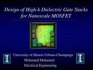
University of Illinois Urbana-Champaign Mohamed Mohamed Electrical Engineering. Design of High-k Dielectric Gate Stacks for Nanoscale MOSFET. Compare and design High-k Dielectric and gate stack using SiO 2

E N D
University of Illinois Urbana-Champaign Mohamed Mohamed Electrical Engineering Design of High-k Dielectric Gate Stacks for Nanoscale MOSFET
Compare and design High-k Dielectric and gate stack using SiO2 Run 2-D Monte Carlo particle Simulation and TCAD drift-diffusion simulation on ‘well tempered’ NMOSFET devices of distinct channel length to analyze the device performance Examine results obtained and understand their correlation to device physics and process engineering Project Goal
General Outline • Background of scaling issues and device engineering • Methodology • Introduction to Numerical Methods • Drift Diffusion TCAD • Monte Carlo • Results • Conclusions and future directions
Scaling Goals & Limitations • Lower cost • Reduce power • Reduce gate delay • Increase operating Frequency • Increase transistor density
Submicron Device Engineering • Source Drain Engineering • Channel Engineering • Retrogrades Profiles • Halo Implants
The need for High-K Dielectric • The need for new generation devices dictates scaling gate dielectric to maximize performance • Tunneling current through SiO2 increases exponentially with decreasing gate oxide thickness
Criteria for High-K Dielectric • Low Leakage current • Thermal Stability • Reliability • Thermal Stability • Good Interface with Si layer • Ability to integrate with metal gate
The Need for Numerical Model in Device Characterization • As technology becomes more complex, the role of accurate simulations tools used for process modeling and design becomes highly needed. • Numerical Models describe the behavior of device by solving charge transport and relevant device equations • Characterize IC design at all levels and at the same time help to cut down product processing time and cost.
Modeling Hierarchy Quantum Transport Boltzmann equation Moments of Boltzmann Equations Hydrodynamic Energy Transport Drift Diffusion Physically based empirical Model
Monte Carlo is used to approximate Mathematical problems by running statistical random sampling on computers. Simulates the motion of a particle (or an electron) with given initial conditions to provide detailed and reliable distributions Objective: Semi-classical approach Direct solution of Boltzmann equation without assumption of distribution function. Monte Carlo
MOCA (Flow Chart) Initialize doping profile Solve Poisson Perform Monte Carlo loop for some femtoseconds of simulation time Monte Carlo Loop displace p and n and Calculate new position Particle experiences Free flight Particle undergoes Some scattering mechanism Perform charge assignment Check contact, Maintain charge Neutrality as needed
Technology Computer Aided Design (TCAD) CAD tool for the simulation of device processing and relevant electrical performance Largely used in device design, providing both decreases in development costs and increases in product quality, reliability, and performance. Drift Diffusion equations: Continuity equations Poisson equation Current equations Drift Diffusion TCAD
Design Approach • Four case analyzed: • Device behavior when all oxide thickness is kept same • SiO2 Device analysis • Device behavior with EOT kept relative to SiO2 • Construction of gate stack that encompasses both SiO2 and high-k
CASE INSULATOR THICKNESS CONSTANT:CONCENTRATION • Parameter • gate doping: 5e20 cm-3 (As n+ polysilicon ) • Leff =25nm; Tox =15 Ao • Substrate Doping: 1e15 cm-3 (B) • Source/Drain Doping: 2.5e20 cm-3. (As) • S/D halo: 2e19 cm-3
CASE: INSULATOR THICKNESS CONSTANT YField for 25nm Device Potenital Plot Vd=0.8V, Vg=0.8
COMPARE ALL : Concentration • high-k device has highest concentration at interface
COMPARE ALL: X EFIELD • Fringing of Field Evident in high-k device
COMPARE ALL: CONDUCTION BAND • Band diagram showing inversion layer as seen in the conduction band
Drift-Diffusion Plot for .05 micron NMOSFET • Higher threshold voltage in SiO2 compared to high-k
Effects of Electric Field • Grid representation of 50nm device (left); Electron current density (right)
ELECTRIC FIELD PLOT ISE-TCAD • High Field seen on oxide silicon interface
Conclusion • Alternative high-k gate-dielectric material for future MOSFET technologies is crucial for device miniaturization and performance requirement. • Increase in gate dielectric thickness leads to more fringing fields that contribute to Short Channel problem. • Overcoming short channel effects in future MOS design is the ultimate challenge in submicron MOS engineering. • Stack Design Produces performance similar to Si02 Dielectric • Advancements of accurate (reliable) TCAD models is crucial in submicron design and analysis.
Future Directions • New approach to device Engineering and novel Materials • Double gate transistors (SOI) • Twice the current • Twice the speed • Room for miniaturization • Carbon Nanotubes
Acknowledgment • Professor Umberto Ravaioli • Professor Swenson • Matt Olson • Dr. Amr Haggag and Gulzar Kathawala • Maneesh Shanbhag
Neuman Boundary Conditions Dirichlet Boundary Conditions Mesh and Free Flight • Monte Carlo Simulates the transport of Particles as a sequence of free flights interrupted by a scattering mechanism • Differential equation describing the device is discretized and used to obtain poisson solutions References: Umberto Ravaiolii and Trudy van der StraatenBeckman Institute