Download
1 / 20
200 likes | 318 Views
Explore the influence of variations in nanoscale VLSI design, from models to sources and beyond. Understand the impact on computing devices such as tablets, smart grids, healthcare, and automotive systems. Discover strategies to mitigate effects and optimize circuit timing and power. Learn about new technologies like 3D ICs and near-threshold computing.

E N D
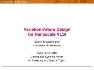
Variation-Aware Design for Nanoscale VLSI Sachin S. Sapatnekar University of Minnesota CAS-FEST 2010 Circuits and Systems Forum on Emerging and Special Topics
The proliferation of computing • Tablets • Entertainment • Smart grid • Healthcare, automotive, security, …
The incredibly shrinking transistor Electronics, Vol. 38, No. 8, Apr 19, 1965
Cost of going to a new technology [GLOBALFOUNDRIES]
So why bother? • Because it makes economic sense… • R&D costs are rising, but so is revenue [GLOBALFOUNDRIES]
Layer 5 Layer 4 Layer 3 Layer 2 Layer 1 Bulk Substrate New technologies: 3D ICs Detailed view Generalized view Interlayer Via Through-silicon Vias (TSVs) SOI wafers with bulk substrate removed Inter-layer bonds 1mm Bulk wafer Metal level of wafer 1 10mm 500mm Device level 1 Adapted from [Das et al., ISVLSI, 2003] by B. Goplen
New technologies: near-threshold computing [Dreslinski et al.]
Types of variations • Based on the model • Systematic • Random • “Random” • Based on the source • Process • Environmental • Design Uncertainty • Based on the time when they are seen • One-time variations • Run-time variations
Channel width variation: poly/ diff rounding, misalignment Gale oxide thickness Random dopant fluctuations Poly Diffusion Uniform Non-uniform Source: S. Tyagi Process-related variations: examples Source: Pey&Tung Source: S. Borkar Many of these variations can be modeled by Gaussians
A taxonomy of variations (contd.) Die-to-Die Wafer-to-Wafer Lot-to-Lot Die-to-Die (D2D) Variations Within-Die (WID) Variations Random Systematic [Intel]
The (f)law of averages [The drunk skater problem] http://www.stanford.edu/~savage/flaw/
Why is this important? • Because it affects circuit timing… • … and power
Si Si Si H H H H2 Gate Oxide Poly Substrate SiH + h+→ Si+ + ½H2 Aging effects • Circuit behaviour degrades with time NBTI Electromigration Oxide breakdown Hot carrier injection • Normal lifetime • Constant failure rate • Based on TDDB, EM, hot-electrons… Failure rate [S. Sjøthun] 1-40 weeks Time 7-15 years [Suto, Teradyne]
Environmental variations • Supply voltage • Soft errors Source: Automotive 7-8, 2004 1
Fried egg By Trubador, available at http://www.phys.ncku.edu.tw/~htsu/humor/fry_egg.html Environmental variations: Temperature [IBM] [Chu 1999] [Joshi] [Intel]
Fried egg Tier 5 Tier 4 Tier 3 Tier 2 By Trubador, available at http://www.phys.ncku.edu.tw/~htsu/humor/fry_egg.html Tier 1 Bulk Substrate Technology trends Detailed view Generalized view Intertier Via [Intel] SOI wafers with bulk substrate removed [Chu 1999] Intertier bonds 1mm Cache 70ºC Bulk wafer Metal level of wafer 1 10mm [Intel] Core 500mm Device level 1 120ºC Adapted from [Das et al., ISVLSI, 2003] [Joshi]
Overcoming variations • Three-pronged strategy • Reduce the fundamental sources • Don’t allow them to be expressed (design around the effects) • Mitigate the effects • Example: temperature effects • Low-power design • Design to reduce T • Design to mitigate T-driven degradation • All all levels of abstraction, using all available methods • Design • CAD • Architecture/OS • Algorithms
Adaptive sensing/mitigation A • Sense/adapt feedback loops • Guardbanded presilicon fixes vs. adaptive postsilicon fixes • Monitor cores • Canary circuits • Silicon odometer • Razor, CRISTA, etc. ... C Phase B PC _ OUT Sensor-driven Comp . ... (freq=fref - fstress) Up to 35% overhead Vdd DC-DC Converter Circuit Block LUT Guardbanding vbp Sensor FBB Generator vbn [Kim, Minnesota]
CAS-FEST 2010 • A Resilience Roadmap • Sani Nassif, IBM • Mitigating Variability in Near-Threshold Computing • Dennis Sylvester, Univ. of Michigan • Robust System Design to Overcome CMOS Reliability Challenges • Subhasish Mitra, Stanford Univ. • Computer Aided Circuit Design for Reliability in Nanometer CMOS • Georges Gielen, Katholieke Univ. – Leuven • Process Compensated High Speed Ring Oscillators in Sub-Micron CMOS • Alyssa B. Apsel, Cornell U. • Containing the Nanometer Pandora-box: Design Techniques for Variation-Aware Low-Power Systems • Abhijit Chatterjee, Georgia Tech.