Download
1 / 15
350 likes | 911 Views
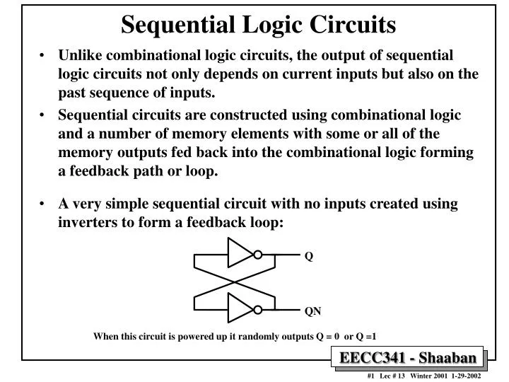
Q. QN. Sequential Logic Circuits. Unlike combinational logic circuits, the output of sequential logic circuits not only depends on current inputs but also on the past sequence of inputs.

E N D
Q QN Sequential Logic Circuits • Unlike combinational logic circuits, the output of sequential logic circuits not only depends on current inputs but also on the past sequence of inputs. • Sequential circuits are constructed using combinational logic and a number of memory elements with some or all of the memory outputs fed back into the combinational logic forming a feedback path or loop. • A very simple sequential circuit with no inputs created using inverters to form a feedback loop: When this circuit is powered up it randomly outputs Q = 0 or Q =1
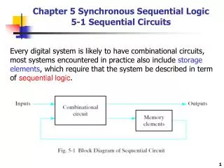
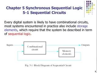
Combinational outputs Memory outputs Combinational logic Memory elements Inputs Sequential Logic Circuits Sequential circuit = Combinational logic + Memory Elements Current State of A sequential Circuit: Value stored in memory elements (value of state variables). State transition: A change in the stored values in memory elements thus changing the sequential circuit from one state to another state.
Q Memory element Memory Element Output: stored single-bit value command Sequential Circuit Buliding Blocks:Generic Memory Elements • A Memory Element: A logic device that can remember a single-bit value indefinitely, or change its value on command from its inputs. • The output Q of the memory element represents the value stored in the memory element. This is also called the state variable of the memory elements. A memory element can be in one of two possible states: • Q = 0 (the memory element has 0 stored), also said be in state 0. • Q =1 (the memory element has 1 stored), also said to be in state 1. • The commands to the memory element formed by its input(s) may include: • Set: Store 1 (Q=1) in the memory element. • Reset: Store 0 (Q=0) in the memory element. • Flip: Change stored value from 0 to 1 or from 1 to 0. • Hold value: Memory value does not change. • Memory Element state transition: A change in the stored value from 0 to 1, or from 1 to 0 such as that caused by a flip command.
The State of A sequential Circuit • A state variable in a sequential circuit represents the single-bit variable Q stored in a memory element in circuit. • Each memory element may be in state 0 or state 1 depending on the current value stored in the memory element. • The State of A sequential Circuit: • The collection of all state variables (memory element stored values) that at any time contain all the information about the past necessary to account for the circuit’s future behavior. • A sequential circuit that contains n memory elements could be in one of a maximum of 2n states at any given time depending on the stored values in the memory elements. • Sequential Circuit State transition: A change in the stored values in memory elements thus changing the sequential circuit from one state to another.
1 Clock signal 0 Clock Cycle Time Falling edges of the clock Rising edges of the clock Clock Signals & Synchronous Sequential Circuits • A clock signal is a periodic square wave that indefinitely switches values from 0 to 1 and 1 to 0 at fixed intervals. • Clock cycle time or clock period: The time interval between two consecutive rising or falling edges of the clock. • Clock Frequency = 1 / clock cycle time(measured in cycles per second or Hz) • Example: Clock cycle time = 1ms clock frequency = 1000Hz • Synchronous Sequential Circuits: Sequential circuits that have a clock signal as one of its inputs: • All state transitions in such circuits occur only when the clock value is either 0 or 1 or happen at the rising or falling edges of the clock depending on the type of memory elements used in the circuit.
Sequential Circuit Memory Elements: Latches, Flip-Flops • Latches and flip-flops are the basic single-bit memory elements used to build sequential circuit with one or two inputs/outputs, designed using individual logic gates and feedback loops. • Latches: • The output of a latch depends on its current inputs and on its previous inputs and its change of state can happen at any time when its inputs change. • Flip-Flop: • The output of a flip-flop also depends on current and previous input but the change in output (change of state or state transition) occurs at specific times determined by a clock input.
Sequential Circuit Memory Elements: Latches, Flip-Flops • Latches: • S-R Latch • S-R Latch With Enable • D-Latch • Flip-Flops: • Edge-Triggered D Flip-Flop • Master/Slave S-R Flip-Flop • Master/Slave J-K Flip-Flop • Edge-Triggered J-K Flip-Flop • T Flip-Flop With Enable
R Q QN S S-R Latch • An S-R (set-reset) latch can be built using two NOR-gates forming a feedback loop. • The output of the S-R latch depends on current as well as previous inputs or state, and its state (value stored) can change as soon as its inputs change. Function Table S R Q QN 0 0 last Q Last QN 0 1 0 1 1 0 1 0 1 1 0 0 Circuit
S Q Enable C QN R S Q C Q R S-R Latch With Enable • Since the S-R latch is responsive to its inputs at all times an enable line C is used to disable or enable state transitions. • Behaves similar to a regular S-R latch when enable C=1 Circuit Function Table S R C Q QN 0 0 1 last Q last QN 0 1 1 0 1 1 0 1 1 0 1 1 1 0 0 x x 0 last Q last QN Logic Symbol
D Q C Q D-Latch • Similar to S-R latch with an enable line, but both S, R are generated from one input D (data) and an inverter. • Stores the value of its input D when enable C =1. C D Q QN 1 0 0 1 1 1 1 0 0 x Last Q Last QN Function Table D Q C QN Logic Symbol Circuit
Master Latch Slave Latch QM D Q D Q D Q QN D Q C Q C Q CLK Q CLK D CLK Q QN 0 0 1 1 1 0 x 0 Last Q Last QN x x Last Q Last QN Clock Circuit Edge-Triggered D Flip-Flop • Uses a pair of D latches and inverters. • Similar in behavior to a D latch except that output and state changes happen at the rising or falling edge of an input clock. • A D Flip-Flop triggered on the rising edge of the clock is given by: Logic Symbol Function Table
Master Latch Slave Latch QM S Q S Q S Q C C QN Q Q R R R CLK S R C Q QN x x 0 last Q last QN 0 0 last Q last QN 0 1 0 1 1 0 1 0 1 1 undef. undef. S Q C Q R Master/Slave S-R Flip-Flop • S-R latches are substituted for the D latches in the negative-edge triggered D flip flop Circuit Function Table Logic Symbol
Circuit Master Latch Slave Latch QM Q S Q S Q J C C QN Q Q R R K CLK J K C Q QN x x 0 last Q last QN 0 0 last Q last QN 0 1 0 1 1 0 1 0 1 1 last QN last Q S Q C Q R Master/Slave J-K Flip-Flop • Solves the problem in the problem when both S=R=1 • When J=K=1 the last state is inverted. Function Table Logic Symbol
Circuit J Q D Q K QN CLK Q CLK J K C Q QN x x 0 last Q last QN x x 1 last Q last QN 0 0 last Q last QN 0 1 0 1 1 0 1 0 1 1 last QN last Q j Q CLK Q k Edge Triggered J-K Flip-Flop • Created from an edge-triggered D flip-flop Logic Symbol Function Table
Q D Q En CLK QN Q T EN T En Q QN x 0 last Q last QN 1 last QN last Q Q j Q T CLK QN Q k T Flip-Flop With Enable • Changes state on every clock cycle (rising edge of T). Circuit OR Function Table