Download
1 / 33
330 likes | 403 Views
Learn about sequential circuits, state tables, state diagrams, and memory components with practical examples and detailed explanations. Understand the importance of states, inputs, and outputs in sequential circuit designs.

E N D
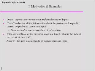
I. Motivation & Examples • Output depends on current input and past history of inputs. • “State” embodies all the information about the past needed to predict current output based on current input. • State variables, one or more bits of information. • If the current State of the circuit is known at time t, what is the state of the circuit at time (t+1) Answer: the next state depends on current state and input
on u u u u u … 1 2 3 4 99 d d d d d I. Motivation & Examples Describing sequential circuit • State table • For each current-state, specify next-states as function of inputs • For each current-state, specify outputs as function of inputs • State diagram • Graphical version of state table Example 1: TV channel control • Let the channel # represent the state of the circuit • Input are up/down on the channel control u: up d: down
I. Motivation & Examples Example 2: A sequential process that inputs an n-bit binary string and outputs 1 if the string contains an even number of 1’s 1 (final output) 01111 SLN 0 (final output) 0111 SLN • What represents the state of the circuit? • Case1: • State as the number of 1’s read so far (possibly infinite # of states) • Case 2: Two states E and O • E (even): if the # of 1’s read so far is even • O (odd) if the # of 1’s read so far is odd
Input Output 1/0 E O 1/1 0/0 0/1 I. Motivation & Examples Example 2: State Diagram for Case 1 Input Output 1/0 1/1 1/0 1/1 1/0 1/1 … 0 1 2 3 4 2n 0/1 0/1 0/1 0/1 0/0 0/0 Example 2: State Diagram for Case 2
Input Output 1/0 E O 1/1 0/0 0/1 I. Motivation & Examples Example 2: State Diagram for Case 2 • Better design • Has less states
I. Motivation & Examples • Example 3: Discuss sequential n-bits comparator • Compare two n-bits numbers X=[Xn-1, …, X0], Y=[Yn-1, …, Y0] • Output 1 if X>Y • Use the basic 1-bit comparator designed in class Shift right ... Xn-1 Xn-2 Xn-3 X2 X1 X0 Operation controlled by a clock to decide: Xi Fi-1 .when to shift input data .when output Fi is stable 1-bit Comparator Ci Yi ... Yn-1 Yn-2 Yn-3 Y2 Y1 Y0 Fi Shift right
I. Motivation & Examples • Example 4: Discuss sequential n-bits adder • Add two n-bits numbers X=[Xn-1, …, X0], Y=[Yn-1, …, Y0] • Output S=X+Y where [Sn,Sn-1,…,S0] • Use the basic 1-bit adder with carry in and carry out Shift right ... Xn-1 Xn-2 Xn-3 X2 X1 X0 Operation controlled by a clock to decide: Xi Ci-1 .when to shift input data .when output are ready 1-bit Full adder Ci Yi ... Yn-1 Yn-2 Yn-3 Y2 Y1 Y0 Ci Shift right Shift right ... Sn Sn-1 Sn-2 S2 S1 S0
Clock signals II. General Representation • Sequential circuit are controlled by a clock signal • Very important with most sequential circuits • State variables change state at clock edge.
General diagram of sequential circuit II. General Representation • Sequential circuit are controlled by a clock signal • Very important with most sequential circuits • State variables change state at clock edge. Input Output i0 i1 … in o0 o1 … om SLN Current states Next states Feedback Memory components State variables: s0,s1, …sk
Some important questions II. General Representation • How to represent the states of a sequential circuit? • How to memorize the (current and next) states? • How to determine the next of the circuit? • How to determine the outputs • as a function F(state) of current state only? • as a function F(input,state) of both input and current state? • The concept of STATE is very important
Memory component II. General Representation • How do we represent the states? • Memory component are used as state variables • Goal: Memorize the current state of the circuit • How are memory components implemented? • Latch, Flip-flop are 1-bit memory component
Bistable element III. Basic memory component • The simplest sequential circuit • Two states • One state variable, say, Q (QN or Q_L the complement of Q) HIGH LOW LOW HIGH
Bistable element III. Basic memory component • The simplest sequential circuit • Two states • One state variable, say, Q LOW HIGH HIGH LOW
Bistable element: Analog analysis III. Basic memory component • Assume pure CMOS thresholds, 5V rail • Theoretical threshold center is 2.5 V
Bistable element: Analog analysis III. Basic memory component • Assume pure CMOS thresholds, 5V rail • Theoretical threshold center is 2.5 V 2.5 V 2.5 V 2.5 V 2.5 V
2.0 V 2.0 V Bistable element: Analog analysis III. Basic memory component • Assume pure CMOS thresholds, 5V rail • Theoretical threshold center is 2.5 V 2.5 V 4.8 V 2.51 V 2.5 V 0.0 V 2.5 V 0.0 V 4.8 V 5.0 V 2.5 V
Bistable element: summary II. General Representation • If (Q=0), then input to Not gate 2 is 0 ==> Output of Not gate 2 is 1 (Q_L =1) ==> The input of Not gate 1 is 1, so output of Not gate 1 is 0 ==> Stable output (Q=0) and (Q_L = 1) • If (Q=1), then input to Not gate 2 is 1 ==> Output of Not gate 2 is 0 (Q_L =0) ==> The input of Not gate 1 is 0, so output Not gate 1 is ==> Stable output (Q=1) and (Q_L = 0) 1 2
Contradiction!!!! S-R Latch…. III. Basic memory component • How to control it? • Screwdriver • Control inputs • S-R latch
S-R Latch…. III. Basic memory component Set operation: SR 00 ----> 10, set the device output to Q=1 regardless of current value of Q Reset operation: SR 00 ----> 01, set the device output to Q=0 regardless of current value of Q Hold operation: SR 10 ----> 00 or 01 ----> 00, Device output are the same as last output values • Only one input value changes • Possible input changes: • SR: 00 ---> 01 ---> 00 ---> 10 ---> 00 …. • Input SR = 11 is not allowed ( Both NOR gates output 0, i.e Q=Q’=0 )
S-R latch operation III. Basic memory component
Progation delay Minimum time to maintain signal at 1 S-R latch timing parameters III. Basic memory component • Propagation delay • Minimum pulse width
S-R latch with enable III. Basic memory component
Input Output i1 o1 in SLN om M1 . . . . . . . . . Mk Sequential network architecture (revisited) III. Basic memory component Components Mi are latches/Flip flops • Operation rules: • Memory components Mi must be in stable state before input changes • Only one input of the component Mi can change at a time
S R q Q Q=q 0 0 0 Hold 0 0 1 Q=0 0 1 0 Reset 0 1 1 Q= 1 1 0 0 Set 1 0 1 1 1 0 Not allowed 1 1 1 III. Basic memory component Charcteristics equation of S-R latch Definition: The characteristic equation specifies a flip-flop next state as a function of its current state and inputs Notation: Let q represent the current state of the flip-flop and Q its next Characteristics table 0 1 0 0 1 1 X X
Q SR 00 01 11 10 q 0 S R q Q X 1 Q=q 1 0 0 0 1 1 X 0 0 1 Q=0 0 1 0 0 1 1 Q= 1 1 0 0 Use K-map method to derive the characteristics equation: Q = S + R’q 1 0 1 1 1 0 1 1 1 III. Basic memory component Charcteristics equation of S-R latch Use the characteristics table to get an excitation map of the flip flop Characteristics table 0 1 0 0 1 1 X X
0 0 to hold current value q ---> Q S R 0 ---> 0 OR 0 X 0 1 to reset Q=0 0 ---> 1 1 0 0 0 to hold current value 1 ---> 0 0 1 1 ---> 1 X 0 OR 1 0 to set Q=1 III. Basic memory component Excitation table of SR flip flop The excitation table describes the input values of S and R that cause the corresponding transitions (q ---> Q) from current to next state Types of transitions: q --->Q 0 ---> 0 0 ---> 1 1 ---> 0 1 ---> 1 Excitation table of S R latch
D latch III. Basic memory component
D-latch operation III. Basic memory component
D-latch timing parameters III. Basic memory component • Propagation delay (from C or D) • Setup time (D before C edge) • Hold time (D after C edge)
Edge-triggered D flip-flop behavior III. Basic memory component
D flip-flop timing parameters III. Basic memory component • Propagation delay (from CLK) • Setup time (D before CLK) • Hold time (D after CLK)