Download
1 / 18
180 likes | 359 Views
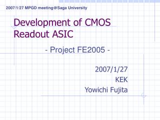
2007/1/27 MPGD meeting @ Saga University. Development of CMOS Readout ASIC. - Project FE2005 -. 2007/1/ 27 KEK Yowichi Fujita. Introduction of FE2005. Features Circuit configuration / Layout Pulse Response Linearity Noise / Timewalk / V TH Variation Summary

E N D
2007/1/27 MPGD meeting@Saga University Development of CMOS Readout ASIC - Project FE2005 - 2007/1/27 KEK Yowichi Fujita
Introduction of FE2005 • Features • Circuit configuration / Layout • Pulse Response • Linearity • Noise / Timewalk / VTH Variation • Summary • The Next Project - FE2006 -
Features • Target: X ray /γray / Neutron Detector • Both positive and negative charge input • CMOS 0.5mm 5V process • Configuration • 8 ch / chip • Input • Preamp:charge amp • Shaper:30ns peaking time • Output • Analog Sum • Digital Out (LVDS) for each channels
Circuit configuration Digital LVDS Out Peaking Time: 30ns Noise: 9000e @CD=100pF Analog Sum Out
Layout 195 mm
Pulse Response Positive Pulse Input Negative Pulse Input Pulse In Pulse In 30ns 30ns Sum Out Sum Out Vth Vth 400mV 400mV LVDS out (differential) LVDS out (differential)
Linearity < 1% INL -1.5pC ~ +1.5pC -1.7pC 1.7pC
VTH Variation • Max. 22mV 22 mV To be improved by Adjusting DAC (each channels)
Timewalk 18 ns 18ns (mean)@Vth = 11fC (equivalent) To be improved by using not Filter out but preamp out
Noise • Measurement • 3,500e @Cd = 1pF • 9,000e @ Cd = 100pF • It’s larger than estimation • Series noise • 60e/pF (40e/pF in estimation) • Parallel noise • ~3000e (1000e in estimation)
Influence from Substrate state Substrate: N-type Potential: VDD Easy to be influenced by substrate state InputPMOS
VDD Dependence Simulation Vsub Dependence VSS Dependence Easy to be influenced by VDD,Vsub To be improved by isolating input MOS from substrate
Summary accomplished accomplished accomplished To be improved To be improved To be improved
FE2005 configuration Digital LVDS Out Peaking Time: 30ns Noise: 9000e @CD=100pF Analog Sum Out
FE2006 Summary Application: X ray/γray/Neutron detector
Schedule • 1/31 Delivery: FE2006 • 2/~ Evaluation: FE2006 • ~ 2/19 Review • 2/20 Design: FE2007 • 3/20 Production • 5/~ Delivery: FE2007