Download
1 / 20
200 likes | 341 Views
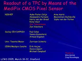
Readout of a TPC using the Medipix2 CMOS pixel sensor. NIKHEF: Alessandro Fornaini Univ. Twente/Mesa+: Harry van der Graaf Jurriaan Schmitz

E N D
Readout of a TPC using the Medipix2 CMOS pixel sensor NIKHEF: Alessandro Fornaini Univ. Twente/Mesa+: Harry van der Graaf Jurriaan Schmitz Jan Timmermans CERN/Medipix Collaboration: Jan Visschers Erik Heijne Peter Kluit Saclay Paul Colas Thanks to: Wim Gotink (CEA/DAPNIA) Ioannis Giomataris Joop Rovenkamp Arnaud Giganon Max Chefdeville (detection of single electrons on a direct pixel segmented anode) LCWS 2004 Paris
Goals • Gas multiplication GEM or Micromegas foil(s) • Charge collection with granularity matching primary ionisation cluster spread • Needs sufficiently low diffusion gas • dE/dx using cluster counting? ( M. Hauschild) • Proof of principle based on existing Medipix2 readout chip LCWS 2004 Paris
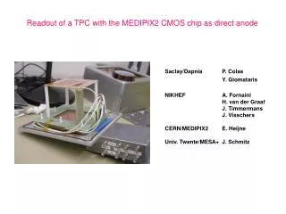
Our GEM-equipped TPC We have constructed a small test TPC equipped with three GEM foils which can be read out by means of theMEDIPIX2 CMOS pixel sensor. The GEM foils were obtained from the CERN/Sauli/GEM group; hole-to-hole distance (hexagonal geometry): 140 µm, hole diameter 85 µm, fiducial surface 100 mm x 100 mm, thickness 50 µm.The drift volume (vol. 100x100x100 mm3) is surrounded by square wire loops, spaced 6.3 mm, put at decreasing potential. Three GEM foils are placed 7.4 mm behind the plane of the bottom wire loop; the distance between GEM foils is 1.6 mm. The anode plane, at ground potential, is 6.6 mm below the third GEM foil. LCWS 2004 Paris
Drift Space GEM foils MediPix CMOS pixel sensor Brass spacer block Printed circuit board Aluminium base plate Drift length: 100 mm Distance between GEMs: 1.6/2.6 mm Distance bottom GEM/MEDIPIX: 6.6 mm Medipix2: 256 x 256 pixels 55 mm x 55 mm area 14 x 14 mm2 each pixel: low-noise preamp, discriminator, two threshold DAC, 13-bit counter, communication logic LCWS 2004 Paris
In the base plate of the chamber, a hole was cut out for the MEDIPIX2 chip: its pixel surface was flush with the (anode plane) base plate plane. The MEDIPIX2 chip contains 256 x 256 square pixels with pitch 55 µm x 55 µm giving a total fiducial sensitive area of 14.08 mm x 14.08 mm. Each pixel is equipped with a low-noise charge preamp, discriminator, two threshold DACs, a 13-bit counter and communication logic.Since a triggering system had not been implemented, we operated the MEDIPIX2 sensor by enabling the counters manually, and stop the counting after a pre-set time interval (0.1 - 10 s). After that, the counts of each pixel are read out. Drift length: 100 mm Distance between GEMs: 1.6/2.6 mm Distance bottom GEM/MEDIPIX: 6.6 mm LCWS 2004 Paris
First events, recorded on March 29, 2003. Drift space irradiated with 55Fe quanta Ar/CH4 90/10 Not immediately understood. Now we do: conversion source ~0.3 mm, defocussing GEM ~0.5 mm, diffusion in driftspace ~1.5 mm LCWS 2004 Paris
No source; exposed 0.01 s No source; exposed 2 s No source; exposed 2 s Feb 9, 2004 Ar/Isobutane 95/5 Fiducial field: 14 x 14 mm2 Collected ionisation in 14 x 14 x 100 mm3 during exposure time LCWS 2004 Paris No source; exposed 0.1 s 90Sr source; exposed 0.01 s
With Paul Colas & Ioannis Giomataris: MediPix2 & Micromegas 55Fe Cathode (drift) plane Drift space: 15 mm Micromegas Baseplate MediPix2 pixel sensor Brass spacer block Printed circuit board Aluminum base plate Very strong E-field above (CMOS) MediPix! LCWS 2004 Paris
MediPix modified by MESA+, Univ. of Twente, The Netherlands Pixel Pitch: 55 x 55 μm2 Bump Bond pad: 25 μm octagonal 75 % surface: passivation SiN New Pixel Pad: 45 x 45 μm2 Insulating surface was 75 % Reduced to 20 % LCWS 2004 Paris
55Fe, 1s No source, 1s 55Fe, 10s 14 mm Friday 13 (!) Feb 2004: signals from a 55Fe source (220 e- per photon); 300 m x 500 m clouds as expected The Medipix CMOS chip faces an electric field of 350 V/50 μm = 7 kV/mm !! Ar/Isobutane 95/5 We always knew, but never saw: the conversion of 55Fe quanta in Ar gas LCWS 2004 Paris
New trial: NIKHEF, March 30 – April 2 Essential: try to see single electrons from cosmic muons (MIPs) Pixel preamp threshold: 3000 e- Required gain: 5000 – 10.000 New Medipix New Micromegas Gas: He/Isobutane 80/20 Ar/Isobutane 80/20 He/CF4 80/20 …… It Works! LCWS 2004 Paris
Prob(n) = 1/G . e-n/G Eff = e-n/G n: threshold setting (#e-) G: Gas amplification LCWS 2004 Paris
He/Isobutane 80/20 Modified MediPix 30 March 2004 LCWS 2004 Paris
He/Isobutane 80/20 Modified MediPix 30 March 2004 LCWS 2004 Paris
He/Isobutane 80/20 Modified MediPix 30 March 2004 LCWS 2004 Paris
He/Isobutane 80/20 Non Modified MediPix Amaricium Source 1 April 2004 LCWS 2004 Paris
He/Isobutane 80/20 Modified MediPix 30 March 2004 LCWS 2004 Paris
He/Isobutane 80/20 Modified MediPix 30 March 2004 LCWS 2004 Paris