Download
1 / 50
520 likes | 907 Views
Introduction to ASIC CMOS and Manufacturing Process. Theerayod Wiangtong Electronic Department Mahanakorn University of Technology. VLSI. Integrated circuits: many transistors on one chip. Very Large Scale Integration (VLSI): very many Complementary Metal Oxide Semiconductor

E N D
Introduction to ASICCMOS and Manufacturing Process Theerayod Wiangtong Electronic Department Mahanakorn University of Technology
VLSI • Integrated circuits: many transistors on one chip. • Very Large Scale Integration (VLSI): very many • Complementary Metal Oxide Semiconductor • Fast, cheap, low power transistors • Today: How to build your own simple CMOS chip • CMOS transistors • Building logic gates from transistors • Transistor layout and fabrication • Rest of the course: How to build a good CMOS chip
Silicon Lattice • Transistors are built on a silicon substrate • Silicon is a Group IV material • Forms crystal lattice with bonds to four neighbors http://jas.eng.buffalo.edu/education/solid/unitCell/home.html
Dopants • Silicon is a semiconductor • Pure silicon has no free carriers and conducts poorly • Adding dopants increases the conductivity • Group V: extra electron (n-type) • Group III: missing electron, called hole (p-type)
p-n Junctions • A junction between p-type and n-type semiconductor forms a diode. • Current flows only in one direction
nMOS Transistor • Four terminals: gate, source, drain, body • Gate – oxide – body stack looks like a capacitor • Gate and body are conductors • SiO2 (oxide) is a very good insulator • Called metal – oxide – semiconductor (MOS) capacitor • Even though gate is no longer made of metal
nMOS Operation • Body is commonly tied to ground (0 V) • When the gate is at a low voltage: • P-type body is at low voltage • Source-body and drain-body diodes are OFF • No current flows, transistor is OFF
nMOS Operation Cont. • When the gate is at a high voltage: • Positive charge on gate of MOS capacitor • Negative charge attracted to body • Inverts a channel under gate to n-type • Now current can flow through n-type silicon from source through channel to drain, transistor is ON
pMOS Transistor • Similar, but doping and voltages reversed • Body tied to high voltage (VDD) • Gate low: transistor ON • Gate high: transistor OFF • Bubble indicates inverted behavior
Power Supply Voltage • GND = 0 V • In 1980’s, VDD = 5V • VDD has decreased in modern processes • High VDD would damage modern tiny transistors • Lower VDD saves power • VDD = 3.3, 2.5, 1.8, 1.5, 1.2, 1.0, …
CMOS Fabrication • CMOS transistors are fabricated on silicon wafer • Lithography process similar to printing press • On each step, different materials are deposited or etched • Easiest to understand by viewing both top and cross-section of wafer in a simplified manufacturing process
Photo-Lithographic Process optical mask oxidation photoresist photoresist coating removal (ashing) stepper exposure Typical operations in a single photolithographic cycle (from [Fullman]). photoresist development acid etch process spin, rinse, dry step http://it.darden.virginia.edu/explore/content/index_frames.htm
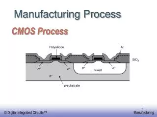
Inverter Cross-section • Typically use p-type substrate for nMOS transistors • Requires n-well for body of pMOS transistors
Well and Substrate Taps • Substrate must be tied to GND and n-well to VDD • Metal to lightly-doped semiconductor forms poor connection called Shottky Diode • Use heavily doped well and substrate contacts / taps
Inverter Mask Set • Transistors and wires are defined by masks • Cross-section taken along dashed line
Detailed Mask Views • Six masks • n-well • Polysilicon • n+ diffusion • p+ diffusion • Contact • Metal
Fabrication Steps • Start with blank wafer • Build inverter from the bottom up • First step will be to form the n-well • Cover wafer with protective layer of SiO2 (oxide) • Remove layer where n-well should be built • Implant or diffuse n dopants into exposed wafer • Strip off SiO2
Oxidation • Grow SiO2 on top of Si wafer • 900 – 1200 C with H2O or O2 in oxidation furnace
Photoresist • Spin on photoresist • Photoresist is a light-sensitive organic polymer • Softens where exposed to light
Lithography • Expose photoresist through n-well mask • Strip off exposed photoresist
Etch • Etch oxide with hydrofluoric acid (HF) • Seeps through skin and eats bone; nasty stuff!!! • Only attacks oxide where resist has been exposed
Strip Photoresist • Strip off remaining photoresist • Use mixture of acids called piranah etch • Necessary so resist doesn’t melt in next step
n-well • n-well is formed with diffusion or ion implantation • Diffusion • Place wafer in furnace with arsenic gas • Heat until As atoms diffuse into exposed Si • Ion Implantation • Blast wafer with beam of As ions • Ions blocked by SiO2, only enter exposed Si
Strip Oxide • Strip off the remaining oxide using HF • Back to bare wafer with n-well • Subsequent steps involve similar series of steps
Polysilicon • Deposit very thin layer of gate oxide • < 20 Å (6-7 atomic layers) • Chemical Vapor Deposition (CVD) of silicon layer • Place wafer in furnace with Silane gas (SiH4) • Forms many small crystals called polysilicon • Heavily doped to be good conductor
Polysilicon Patterning • Use same lithography process to pattern polysilicon
Self-Aligned Process • Use oxide and masking to expose where n+ dopants should be diffused or implanted • N-diffusion forms nMOS source, drain, and n-well contact
N-diffusion • Pattern oxide and form n+ regions • Self-aligned process where gate blocks diffusion • Polysilicon is better than metal for self-aligned gates because it doesn’t melt during later processing
N-diffusion cont. • Historically dopants were diffused • Usually ion implantation today • But regions are still called diffusion
N-diffusion cont. • Strip off oxide to complete patterning step
P-Diffusion • Similar set of steps form p+ diffusion regions for pMOS source and drain and substrate contact
Contacts • Now we need to wire together the devices • Cover chip with thick field oxide • Etch oxide where contact cuts are needed
Metalization • Sputter on aluminum over whole wafer • Pattern to remove excess metal, leaving wires
Layout • Chips are specified with set of masks • Minimum dimensions of masks determine transistor size (and hence speed, cost, and power) • Feature size improves 30% every 3 years or so • Normalize for feature size when describing design rules
Design Rules • Interface between designer and process engineer • Guidelines for constructing process masks • Unit dimension: Minimum line width • scalable design rules: lambda parameter • absolute dimensions (micron rules)
Layer Color Representation Well (p,n) Yellow Active Area (n+,p+) Green Select (p+,n+) Green Polysilicon Red Metal1 Blue Metal2 Magenta Contact To Poly Black Contact To Diffusion Black Via Black CMOS Process Layers
Intra-Layer Design Rules 4 Metal2 3
Design Rule Checker poly_not_fet to all_diff minimum spacing = 0.14 um.
V DD 3/1 Out In 1/1 GND Stick diagram of inverter Sticks Diagram • Dimensionless layout entities • Only topology is important • Final layout generated by “compaction” program