Download
1 / 1
10 likes | 150 Views
Effects of Surrounding Materials on Proton-Induced Energy Deposition in Large Silicon Diode Arrays. Christina L. Howe 1 , Robert A. Weller 1 , Robert A. Reed 1 , Brian D. Sierawski 2 , Paul W. Marshall 3 , Cheryl J. Marshall 4 , Marcus H. Mendenhall 1 ,

E N D
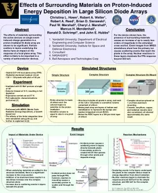
Effects of Surrounding Materials on Proton-Induced Energy Deposition in Large Silicon Diode Arrays Christina L. Howe1, Robert A. Weller1, Robert A. Reed1, Brian D. Sierawski2, Paul W. Marshall3, Cheryl J. Marshall4, Marcus H. Mendenhall1, Ronald D. Schrimpf1, and John E. Hubbs5 Abstract Conclusion The effects of materials surrounding the active devices on single event-induced charge generation in a proton-irradiated Si diode array are shown to be significant. Particle scatters in layers underlying the device have an impact on the response of a focal plane array. This effect is likely to be important in a variety of semiconductor devices. For the device shown here, the presence of surrounding materials causes an increase of up to nearly two-orders of magnitude in the simulated cross section. Event images from MRED simulations show how the primary ion causes scattering events that reach the pixels in the array. Nuclear reactions in these layers dominate the FPA response beyond 500 keV. • Vanderbilt University, Department of Electrical Engineering and Computer Science • Vanderbilt University, Institute for Space and Defense Electronics • Consultant • NASA/GSFC • Ball Aerospace and Technologies Corp Device Simulated Structures • Hybrid Si P-i-N focal plane array (FPA) • Radiation-hardened readout circuit • 128 × 128 pixels with pitch of 60 µm Complex Structure Complex Structure On Mount Simple Structure Experiment • Irradiated with 63 MeV protons at angle of 45° • Detector biased at 15 V, resulting in full depletion • Exposures carried out at 277 K • Full radiometric characterizations performed [1] • Entire structure is made of silicon and the colored region is sensitive to the proton irradiation • Sensitive volume is equal in size to one pixel of array • Structure includes all pixels in array, and each of the 128 x 128 pixels is a sensitive volume comprised of silicon • Below pixel array are layers of indium and metallization to represent the bumps and readout integrated circuit (ROIC) • Below the ROIC layers is a 300 µm thick layer of silicon • Complex structure placed on 1 cm thick aluminum mounting • Ceramic, beryllium, copper, and tantalum mounts were also considered, all showed approximately the same result Simulation • Performed with MRED (Monte Carlo Radiative Energy Deposition), a Geant4 based tool • The effects of the finite integration time were simulated using pile up, and further in explained in [2] Results Event Images Impact of Materials Under Device Reaction Mechanisms • Incident proton causes a scattering event in layers directly beneath pixels • A secondary proton is created which then passes through other pixels and deposits energy • When underlying materials are added to the structure simulated, there is a significant increase in the cross section • Addition of an aluminum base results in a two-times increase over the complex structure alone • Increase due to scattering events in layers beneath the pixels • Scattering events in the layers underneath the pixels in the complex device result in energy deposition from direct ionization • Nuclear reactions begin to dominate the response around 420 keV for the simple structure, and 450 keV for the complex structure • Incident proton does not pass through FPA, however, reaction in mounting causes a secondary proton to scatter and through the FPA [1] J. E. Hubbs et al., Proc. SPIE, vol. 5902, 2005. [2] C. L. Howe et al., IEEE Trans. Nucl. Sci., vol. 54, 2007.