Download
1 / 2
20 likes | 45 Views
Our team knows how to get you the best silicon wafer, regardless of shape, size, and function. If you are interested in purchasing wafers, please email us at sales@waferworld.com.

E N D
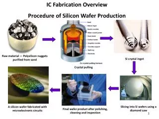
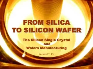
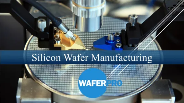
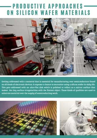
PRODUCTIVE APPROACHES ON SILICON WAFER MATERIALS Getting addressed with a material that is essential for manufacturing over semiconductors found on all kinds of electronic devices. It exposes a chance to encounter using a silicon wafer in daily life. This gets addressed with an ultra-flat disk which is polished to reflect as a mirror surface that makes the tiny surface irregularities with the flattest object. These kinds of qualities are used to substrate material over the supply of semiconducting work.
PACKAGING METHODS GENERAL VIEW These silicon-based materials are exposed to more abundant elements to use in various things. The most common material that holds silicon is quartz, agate, flint is done in more concerning connections. It also makes a common material on producing semiconductors and microchips which does not conduct the resistivity process over exact specification. Viewing over silicon prices then it gets the growth of arranged atoms in a three-dimensional periodic pattern that extends over entire material with different orientation works. Once these wafers are completely arranged with final cleaning steps where engineers give some specification and inspection on leaving high intensity done with the laser scanning process. It detects certain an unwanted particles along with some defects that occurred during fabrication are cleared. All of these wafers leave on making proper specifications in cassettes and sealed tapes are done in silicon. SLICING PROCESS INNOVATION PROGRESSION After the ingot is completely grown that is ground to make rough size with a targeting size of a final silicon wafer. These things create a notch or flat cut to indicate its entire orientation after passing huge variation on inspection for undergoing slicing works. Once the wafers are sliced, the lapping process begins to remove saw marks and gets a defect in front as well as the backside of wafers. It gets a thin surface to relieve stress an accumulated in wafer over slicing process which can go through etching and cleaning works to be done in a delighted manner. Involving of sodium hydroxide or other chemical alleviate any microscopic cracks along with any of those minute damages are resolved in lapping works. Day to day life arranges to see silicon wafer that is used in every sort of electronic device over indispensable living things. All sort of access these technological innovation gets addressed on enabled for the process evolutionary development over electronic devices makes immeasurable functions to our lives. Some of these products as give consequent supply that is used in smaller as well as a stronger impact on a product. It goes beyond achievements in making revolutionary changes done on silicon material. CLEANING FUNCTIONALITY Getting involved final as well as a crucial step in the manufacturing process is done with a polishing wafer. It makes complete functionality makes ranges from an entire process. These kinds of particles are not visible in the naked eye where it addresses with an uncontrolled atmosphere that sets on maintaining a level of cleanliness. Focusing on polishing works that are progressively exposed with finer slurries through polishing compounds. The majority of them are polished on the front phase gives a mirror finish that makes distinguish to use for device fabrications. (561) 842-4441 Palm Beach, FL 33407