Download
1 / 52
520 likes | 631 Views
Frekvencijske karakteristike elektronskih kola. Prenosne funkcije (nule i polovi) Amplitudno-frekvencijski i fazno-frekvencijski dijagrami. Frekvencijski nezavisno kolo Pojacanje A ne zavisi od f. Frekvencijski zavisno kolo primjer 1.

E N D
Frekvencijske karakteristike elektronskih kola Prenosne funkcije (nule i polovi) Amplitudno-frekvencijski i fazno-frekvencijski dijagrami
Ucestanost (frekvencija) sNulta ucestanost s=0Realna ucestanost s=jw
Kada u A(s) stavimo s=jw, dobijamo prenosnu funkciju za realne ucestanosti A(jw)
Kompleksno pojacanje A(jw) Vul(t) Viz(t)
Logaritamsko pojacanje AdB • A= 0.001 AdB= -60dB • A=0.01 AdB= -40dB • A=0.1 AdB= -20dB • A=1/2 AdB= -6dB • A=1 AdB= 0dB • A=2 AdB= +6dB • A=10 AdB= +20dB • A=100 AdB= +40dB
Fig.1.23(a) Magnitude and (b) phase response of STC networks of the low-pass type.
Fig. 7.1 Bode plot for the typical magnitude term. The curve shown applies for the case of a zero. For a pole, the high-frequency asymptote should be drawn with a 6-dB/octave slope.
Fig.1.24(a) Magnitude and (b) phase response of STC networks of the high-pass type.
Fig. 7.3 Bode plot of the typical phase term tan-1 (/a) when a is negative.
Konjugovano kompleksni par nula blizu jw ose unosi rezonantno ulegnuce i strmiju promjenu faze
Analiza frekvencijskih karakteristika • Nalazenje prenosne funkcije kola • Nalazenje nula i polova ove funkcije • Crtanje AF i FF dijagrama
Nalazenje prenosne funkcije kola • Elektronske komponente (tranzistore, diode, itd) zamjenimo modelima za male signale i svodimo problem na linearno kolo sa koncentrisanim parametrima. • Reaktanse uvijek donose polove.
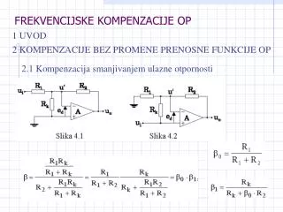
Kondenzator u otocnoj grani donosi nulu kada je vezan na red sa otpornikom.
Induktivnost u otocnoj grani donosi nulu. • Induktivnost u direktnoj grani donosi nulu kada je na red vezana sa otpornikom. • Ucestanost pola Sp=-1/t, gdje je t=C*Re, gdje je Re ekvivalentna otpornost koju “vidi” kondenzator. • Analogno t=L/Re, gdje je Re otpornost koju “vidi” induktivitet.
Fig. 7.13 The classical common-emitter amplifier stage. (The nodes are numbered for the purposes of the SPICE simulation in Example 7.9.)
Fig. 7.14 Equivalent circuit for the amplifier of Fig. 7.13 in the low-frequency band.
Fig. 7.33 Variation of (a) common-mode gain, (b) differential gain, and (c) common-mode rejection ratio with frequency.
Fig. 11.3 Specification of the transmission characteristics of a low-pass filter. The magnitude response of a filter that just meets specifications is also shown.
Fig. 11.4 Transmission specifications for a bandpass filter. The magnitude response of a filter that just meets specifications is also shown. Note that this particular filter has a monotonically decreasing transmission in the passband on both sides of the peak frequency.
Fig. 11.5 Pole-zero pattern for the low-pass filter whose transmission is sketched in Fig.11.3. This filter is of the fifth order (N = 5.)
Fig. 11.6 Pole-zero pattern for the bandpass filter whose transmission is shown in Fig.11.4. This filter is of the sixth order (N = 6.)
Fig. 11.9 Magnitude response for Butterworth filters of various order with = 1. Note that as the order increases, the response approaches the ideal brickwall type transmission.
Fig. 11.10 Graphical construction for determining the poles of a Butterworth filter of order N. All the poles lie in the left half of the s-plane on a circle of radius 0 = p(1/)1/N, where is the passband deviation parameter : (a) the general case, (b)N = 2, (c)N = 3, (d)N = 4.
Fig. 11.12 Sketches of the transmission characteristics of a representative even- and odd-order Chebyshev filters.
Fig. 11.18 Realization of various second-order filter functions using the LCR resonator of Fig.11.17(b): (a) general structure, (b) LP, (c) HP, (d) BP, (e) notch at 0, (f) general notch, (g) LPN (n0), (h) LPN as s , (i) HPN (n < 0).
Fig. 11.20(a) The Antoniou inductance-simulation circuit. (b) Analysis of the circuit assuming ideal op amps. The order of the analysis steps is indicated by the circled numbers.
Fig. 11.22a Realizations for the various second-order filter functions using the op amp-RC resonator of Fig.11.21(b). (a) LP; (b) HP; (c) BP, (d) notch at 0;
Fig.11.22b(e) LPN, n0; (f) HPN, n0; (g) all-pass. The circuits are based on the LCR circuits in Fig.11.18. Design equations are given in Table11.1.
Fig. 11.25 Derivation of an alternative two-integrator-loop biquad in which all op amps are used in a single-ended fashion. The resulting circuit in (b) is known as the Tow-Thomas biquad.