Download
1 / 26
260 likes | 398 Views
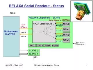
The RELAXd Serial Readout System features a MASTER-SLAVE communication protocol, capable of transferring data at speeds up to 600 Mbps for multi-pixel chips like MPix. This system uses Lattice SC15 FPGA technology to handle control commands and data transmission, offering support for external inputs such as shutters. It operates with 16-bit words and implements effective data handling using 8b/10b encoding. Key functionalities include a robust state management system for various operational modes, ensuring reliable data accuracy and control.

E N D
RELAXd Serial Readout - Status Idea: RELAXd Chipboard – SLAVE Motherboard MASTER Serial data up to 600Mbps MPix0 FPGA LatticeSC15 up to 3Gbps control MPix1 serial MPix2 8b/10b MPix3 Ext. inputs (ext. shutter etc.) ADC DACs Flash Power SLAVE 2 SLAVE 3 etc. RELAXd Serial Readout Status
Master – Slave Communication Protocol Commands/data sent from Master to Slave Data sent from Slave/MPix to Master 16bit words 16bit words SOP SOP Header Header Index++, length Index++, length Command ID Data Command Command Parameters/Data Trailer CRC EOP Trailer CRC EOP • Only one command (Mpix_Mode, Read_Status, Set_Config, Set_Int_DAQ) • in each command block (no command list necessary) RELAXd Serial Readout Status
Implementation - Schematics of Data Path 150 MHz 600 MHz 3GHz 1b 4b SDR_Out_0 delay0 SDR SM 1b 4b PCS 8b/10b Pcs_Out SM FIFO_Out 16b x 512 delay1 SDR_Out_1 16b Data_Out 1b 16b 16b 1b 4b delay2 SDR_Out_2 1b 4b to MPix Quad delay3 SDR_Out_3 to Master 1b 4b SDR_In_0 1b 4b Pcs_In SM FIFO_In 16b x 512 SDR_In_1 16b 1b 16b 16b Data_In 1b 4b SDR_In_2 1b 4b SDR_In_3 M0, M1,Shutter, Enable_In, Reset SM reset Enable_out 130MHz Int. DAQ Control SM DLL fClock_in OSCA PLL FPGA Ext_clk reset Ext_shutter type TX_STATE_TYPE is (IDLE, SENDING_DATA); type RX_STATE_TYPE is (ERROR, IDLE, READING_DATA, M_RESET); type MPIX_STATE_TYPE is (ERROR, IDLE, READ_COMMAND, SET_MPIX_MODE, SETTING_MATRIX, READING_MATRIX, SETTING_DACS, COUNTING, RESETTING_MATRIX); RELAXd Serial Readout Status
SDR Block – gearing 4 to 1 Channel data_out to fast_clock alignment RELAXd Serial Readout Status
Clock Path (backup) FPGA 150 MHz 600 MHz 3GHz 1b SDR_Out_0 delay0 SDR SM 1b PCS 8b/10b Pcs_Out SM FIFO_Out 16b x 512 delay1 SDR_Out_1 Data_Out 1b delay2 SDR_Out_2 1b to MPix Quad delay3 SDR_Out_3 to Master tx_refClk 1b SDR_In_0 1b Pcs_In SM FIFO_In 16b x 512 SDR_In_1 Data_In 1b SDR_In_2 rx_clk 1b SDR_In_3 rx_refClk M0, M1,Shutter, Enable_In, Reset 130MHz Enable_out DIV/4 sClk OSCA fClk DLL fClock_in PLL Ext_clk reset Ext_shutter RELAXd Serial Readout Status
Clock Path (baseline) FPGA 150 MHz 600 MHz 3GHz 1b SDR_Out_0 delay0 SDR SM 1b PCS 8b/10b Pcs_Out SM FIFO_Out 16b x 512 delay1 SDR_Out_1 Data_Out 1b delay2 SDR_Out_2 1b to MPix Quad delay3 SDR_Out_3 to Master tx_refClk 1b SDR_In_0 1b Pcs_In SM FIFO_In 16b x 512 SDR_In_1 Data_In 1b SDR_In_2 rx_clk 1b SDR_In_3 M0, M1,Shutter, Enable_In, Reset rx_refClk PLL_ref Enable_out DIV/4 sClk PLL fClk OSCA DLL fClock_in 130MHz Ext_clk reset Ext_shutter RELAXd Serial Readout Status
FPGA Inputs/Outputs -- CMOS medipix mpix_reset: out std_logic; -- active low! mpix0_shutter: out std_logic; -- or common to all? mpix1_shutter: out std_logic; mpix2_shutter: out std_logic; mpix3_shutter: out std_logic; mpix_M: out std_logic_vector(1 downto 0); --- mpix0_spareFSR: out std_logic; -- only in mpix2.1 --- mpix1_spareFSR: out std_logic; --- mpix2_spareFSR: out std_logic; --- mpix3_spareFSR: out std_logic; mpix_polarity: out std_logic; mpix_p_s: out std_logic; --set to 0 !! mpix_enable_tpulse: out std_logic; -- pcs serial inputs/outputs pcs_hdinp_0, pcs_hdinn_0 : in std_logic; pcs_hdoutp_0, pcs_hdoutn_0 : out std_logic ); end; entity top is port ( -- CMOS global_reset: in std_logic; -- reset button ? ext_clk: in std_logic; -- clock from ext. oscilator ext_shutter: in std_logic; -- LVDS medipix mpix0_data_in: out std_logic; mpix1_data_in: out std_logic; mpix2_data_in: out std_logic; mpix3_data_in: out std_logic; mpix0_fclock_in: out std_logic; mpix1_fclock_in: out std_logic; mpix2_fclock_in: out std_logic; mpix3_fclock_in: out std_logic; mpix0_enable_in: out std_logic; mpix1_enable_in: out std_logic; mpix2_enable_in: out std_logic; mpix3_enable_in: out std_logic; mpix0_data_out: in std_logic; mpix1_data_out: in std_logic; mpix2_data_out: in std_logic; mpix3_data_out: in std_logic; mpix0_enable_out: in std_logic; mpix1_enable_out: in std_logic; mpix2_enable_out: in std_logic; mpix3_enable_out: in std_logic; ADC/DAC/Power IO not included yet! Total: LVDS I/O - 8/12 + serdes 1/1 CMOS I/O - > 3/10 RELAXd Serial Readout Status
FPGA Inputs/Outputs notes: • Serdes CH0, for debugging maybe also useful another channel (CH1) • external shutter • Ref clock (CMOS ?) • Reset and Load_Config buttons • would be nice to have some probe pins (2 to 4 ?) • additional switches (2 ?) • and status LEDs (4 ?) • DAC/ADS/Power chip IO’s … • something else ??? RELAXd Serial Readout Status
SC15 IO Data Sheet • Fpga LatticeSC15 – 139 IO pins, 4 SERDES, 17x17mm (256-ball fpBGA pack). RELAXd Serial Readout Status
1 2 7 3 6 RELAXd Serial Readout Status 5 4
FPGA SC15 Utilization RELAXd Serial Readout Status
FPGA SC15 Power Calculation RELAXd Serial Readout Status
Test Bench Setup – SC25 Evaluation Board LatticeSCM Evaluation Board FPGA 3GHz OSCA Clk_130MHz 600 MHz 1b 150 MHz 4b SDR_Out_0 SDR_Out SM 1b 16b 4b PCS 8b/10b Pcs_Out SM FIFO_Out 16b x 512 SDR_Out_1 1b 16b 16b 16b 1b 4b SDR_Out_2 1b 4b SDR_Out_3 to Master 1b 4b SDR_In_0 SDR_In SM 1b 4b 16b Pcs_In SM FIFO_In 16b x 512 SDR_In_1 1b 16b 16b 1b 4b SDR_In_2 1b 4b SDR_In_3 to MPix Reset_bypass fClock MPix Control SM 1b PCS m “Master” Control Emulator Jtag_Tracy “Logic Analyzer” Command Status Registers 16b x 16 SWITCHES Tracy FIFO Command SM 1b Out pins, LED’s PCS ethernet Jtag-USB Marvell Ethernet Board ethernet RELAXd Serial Readout Status
Current Test Setup:LatticeSC Evaluation Board + Medipix (one chip) RELAXd Serial Readout Status
Measured speed without errors FPGA I/O only: > 532 MHz (higher not tested yet), Master-Slave 2.66 Gbit/s; Medipix 2.1: • Fast Shift Register – 266 MHz (FSR test mode) • Set/Read matrix – 83 MHz ok (100 MHz with a data shift in bits 0 of pixel row 0 and errors in the last pixel column) ; Medipix MXR (with default DAC settings): • FSR – 166 MHz (matrix setting mode) • S/R matrix – 100 MHz ok, 166 MHz with errors in the last or first column; • should be faster when better DAQ (lvds) settings loaded (not tested yet) • fast 8b/10b serial link and communication between Lattice SC FPGA and Medipix work. RELAXd Serial Readout Status
FPGA SC25 Eval Board Utilization RELAXd Serial Readout Status
FPGA SC25 Eval Board Power Calculation RELAXd Serial Readout Status
Planned Test Bench with Slave Board Lattice SC15 FPGA EPROM FLEX ? C C SMA V-bias ADC DAC PWR JTAG Slave board prototype Standard serial < 3.4 Gbits/s 8b/10b (clock encoded in data) Marvell ethernet board ethernet Lattice SC Evaluation board (“master”) RELAXd Serial Readout Status
To Do: • Designing the Slave board prototype and Quad chip carrier (see Bas v.d. Heijden talk) • 10 Lattice SC15 Fpga’s already received (see pic); • Connect the Lattice evaluation board with PC over ethernet via Marvell board and get FPGA-SDRAM interface running, so eval. board can be used as “master” for a slave board evaluation. (Marvell board already in our hands.) • Complete the firmware for slave board. • Test clock scheme using rx_clock from Master! • PCS checksum, FIFO setup/hold time, SDR internal DAQ, external shutter • Error handling etc. RELAXd Serial Readout Status