
80C196KB Memory Map and Peripheral Overview
This document details the memory map, special function registers, and peripheral overview of the 80C196KB microcontroller, including PWM, timers, HSIO, serial port, and A/D converter.
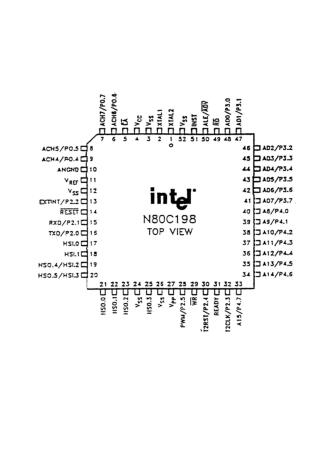

80C196KB Memory Map and Peripheral Overview
E N D
Presentation Transcript
80C196KB Memory Map 80C196KB Special Function Registers
80C196KB Block Diagram 80C196KB Block diagram
There are two bytes in the PSW; the actual status word and the low byte of the interrupt mask. Figure 3-1 shows the status bits of the PSW. The PSW can be saved in the system stack with a single operation (PUSHF) and restored in a like manner (POPF). Only the interrupt section of the PSW can be accessed directly. There is no SFR for the PSW status bits.
4.0 PERIPHERAL OVERVIEW There are five major peripherals on the 80C196KB: the pulse-width-modulated output (PWM), Timer1 and Timer2, High Speed I/O Unit, Serial Port and A/D Converter. With the exception of the high speed I/O unit (HSIO), each of the peripherals is a single unit that can be discussed without further separation. Four individual sections make up the HSIO and work together to form a very flexible timer/counter based I/O system. Included in the HSIO are a 16-bit timer (Timer1), a 16-bit up/down counter (Timer2), a programmable high speed input unit (HSI), and a programmable high speed output unit (HSO). With very little CPU overhead the HSIO can measure pulse widths, generate waveforms, and create periodic interrupts. Depending on the application, it can perform the work of up to 18 timer/counters and capture/compare registers. A brief description of the peripheral functions and interractions is included in this section. It provides overview information prior to the detailed discussions in the following sections. All of the details on control bits and precautions are in the individual sections for each peripheral starting with Section 5. 4.1 Pulse Width Modulation Output (D/A) Digital to analog conversion can be done with the Pulse Width Modulation output. The output waveform is a variable duty cycle pulse which repeats every 256 state times or 512 state times if the prescaler is enabled. Changes in the duty cycle are made by writing to the PWM register. There are several types of motors which require a PWM waveform for most efficient operation. Additionally, if this waveform is integrated it will produce a DC level which can be changed in 256 steps by varying the duty cycle. Details on the PWM are in Section 6.
4.2 Timers Two 16-bit timers are available for use on the 80C196KB. The first is designated ``Timer1'', the second ``Timer2''. Timer1 is used to synchronize events to real time, while Timer2 is clocked externally and synchronizes events to external occurrences. The timers are the time bases for the High Speed Input (HSI) and High Speed Output (HSO) units and can be considered an integral part of the HSI/O. Details on the timers are in Section 7. Timer1 is a free-running timer which is incremented every eight state times, just as it is on the 8096BH. Timer1 can cause an interrupt when it overflows. Timer2 counts transitions, both positive and negative, on its input which can be either the T2CLK pin or the HSI.1 pin. Timer2 can be read and written and can be reset by hardware, software or the HSO unit. It can be used as an up/down counter based on Port 2.6 and it's value can be captured into the T2CAPture register. Interrupts can be generated on capture events and if Timer2 crosses the 0FFFFH/0000H boundary or the 7FFFH/8000H boundary in either direction. 4.3 High Speed Inputs (HSI) The High Speed Input (HSI) unit can capture the value of Timer1 when an event takes place on one of four input pins (HSI.0-HSI.3). Four types of events can trigger a capture: rising edges only, falling edges only, rising or falling edges, or every eighth rising edge. A block diagram of this unit is shown in Figure 4-3. Details on the HSI unit are in Section 8. When events occur, the Timer1 value gets stored in the FIFO along with 4 status bits which indicate the input line(s) that caused the event. The next event ready to be unloaded from the FIFO is placed in the HSI Holding Register, so a total of 8 pieces of data can be stored in the FIFO. Data is taken off the FIFO by reading the HSI–STATUS register, followed by reading the HSI–TIME register. When the time register is read the next FIFO location is loaded into the holding register.
Three forms of HSI interrupts can be generated: when a value moves from the FIFO into the holding register; when the FIFO (independent of the holding register) has 4 or more events stored; and when the FIFO has 6 or more events stored. This flexibility allows optimization of the HSI for the expected frequency of interrupts. Independent of the HSI operation, the state of the HSI pins is indicated by 4 bits of the HSI–STATUS register. Also independent of the HSI operation is the HSI.0 pin interrupt, which can be used as an extra external interrupt even if the pin is not enabled to the HSI unit. 4.4 High Speed Outputs (HSO) The High Speed Output (HSO) unit can generate events at specified times or counts based on Timer1 or Timer2 with minimal CPU overhead. A block diagram of the HSO unit is shown in Figure 4-4. Up to 8 pending events can be stored in the CAM (Content Addressable Memory) of the HSO unit at one time. Commands are placed into the HSO unit by first writing to HSO– COMMAND with the event to occur, and then to HSO–TIME with the timer match value. Fourteen different types of events can be triggered by the HSO: 8 external and 6 internal. There are two interrupt vectors associated with the HSO, one for external events, and one for internal events. External events consist of switching one or more of the 6 HSO pins (HSO.0-HSO.5). Internal events include setting up 4 Software Timers, resetting Timer2, and starting an A/ D conversion. The software timers are flags that can be set by the HSO and optionally cause interrupts. Details on the HSO Unit are in Section 9. 4.5 Serial Port The serial port on the 80C196KB is functionally compatible with the serial port on the MCS-51 and MCS-96 families of microcontrollers.
One synchronous and three asynchronous modes are available. The asynchronous modes are full duplex, meaning they can transmit and receive at the same time. Double buffering is provided for the receiver so that a second byte can be received before the first byte has been read. The transmitter is also double buffered, allowing bytes to be written while transmission is still in progress. The Serial Port STATus (SP–STAT) register contains bits to indicate receive overrun, parity, and framing errors, and transmit and receive interrupts. Details on the Serial Port are in Section 10. MODES OF OPERATION Mode 0 is a synchronous mode which is commonly used for shift register based I/O expansion. Sets of 8 bits are shifted in or out of the 80C196KB with a data signal and a clock signal. Mode 1 is the standard asynchronous communications mode: the data frame used in this mode consists of 10 bits: a start bit (0), 8 data bits (LSB first), and a stop bit (1). Parity can be enabled to send an even parity bit instead of the 8th data bit and to check parity on reception. Modes 2 and 3 are 9-bit modes commonly used for multi-processor communications. The data frame used in these modes consist of a start bit (0), 9 data bits (LSB first), and a stop bit (1). When transmitting, the 9th data bit can be set to a one to indicate an address or other global transmission. Devices in Mode 2 will be interrupted only if this bit is set. Devices in Mode 3 will be interrupted upon any reception. This provides an easy way to have selective reception on a data link. Mode 3 can also be used to send and receive 8 bits of data plus even parity. BAUD RATES Baud rates are generated in an independent 15-bit counter based on either the T2CLK pin or XTAL1 pin. Common baud rates can be easily generated with standard crystal frequencies. A maximum baud rate of 750 Kbaud is available in the asynchronous modes with 12MHz on XTAL1. The synchronous mode has a maximum rate of 3.0 Mbaud with a 12 MHz clock.
4.6 A/D Converter The 80C196KB's Analog interface consists of a sample and-hold, an 8-channel multiplexer, and a 10-bit successive approximation analog-to-digital converter. Analog signals can be sampled by any of the 8 analog input pins (ACH0 through ACH7) which are shared with Port 0. An A/D conversion is performed on one input at a time using successive approximation with a result equal to the ratio of the input voltage divided by the analog supply voltage. If the ratio is 1.00, then the result will be all ones. A conversion can be started by writing to the A/D–Command register or by an HSO Command. Details on the A/D converter are in Section 11. 4.7 I/O Ports There are five 8-bit I/O ports on the 80C196KB. Some of these ports are input only, some are output only, some are bidirectional and some have multiple functions. In addition to these ports, the HSI/O pins can be used as standard I/O pins if their timer related features are not needed. Port 0 is an input port which is also the analog input for the A/D converter. Port 1 is a quasi-bidirectional port and the 3MSBs of Port 1 are multiplexed with the HOLD/HLDA functions. Port 2 contains three types of port lines: quasi-bidirectional, input and output. Its input and output lines are shared with other functions such as serial port receive and transmit and Timer2 clock and reset. Ports 3 and 4 are open-drain bidirectional ports which share their pins with the address/data bus. Quasi-bidirectional pins can be used as input and output pins without the need for a data direction register. They output a strong low value and a weak high value. The weak high value can be externally pulled low providing an input function. A detailed explanation of these ports can be found in Section 12.
4.8 Watchdog Timer The Watchdog Timer (WDT) provides a means to recover gracefully from a software upset. When the watchdog is enabled it will initiate a hardware reset unless the software clears it every 64K state times. Hardware resets on the 80C196KB cause the RESET input pin to be pulled low, providing a reset signal to other components on the board. The WDT is independent of the other timers on the 80C196KB. 5.0 INTERRUPTS Twenty-eight (28) sources of interrupts are available on the 80C196KB. These sources are gathered into 15 vectors plus special vectors for NMI, the TRAP instruction, and Unimplemented Opcodes. Figure 5-1 shows the routing of the interrupt sources into their vectors as well as the control bits which enable some of the sources. Special Interrupts Three special interrupts are available on the 80C196KB: NMI, TRAP and Unimplemented opcode. The external NMI pin generates an unmaskable interrupt for implementation of critical interrupt routines. The TRAP instruction is useful in the development of custom software debuggers or generation of software interrupts. The unimplemented opcode interrupt generates an interrupt when unimplemented opcodes are executed. This provides software recovery from random execution during hardware and software failures. Although available for customer use, these interrupts may be used in Intel development tools or evaluation boards. NMI NMI, the external Non-Maskable Interrupt, is the highest priority interrupt. It vectors indirectly through location 203EH. For design symmetry, a mask bit exists in INT–MASK1 for the NMI.
To prevent accidental masking of an NMI, the bit does not function and will not stop an NMI from occurring. For future compatibility, the NMI mask bit must be set to zero. NMI on the 8096 vectored directly to location 0000H, so for the 80C196KB to be compatible with 8096 software, which uses the NMI, location 203EH must be loaded with 0000H. The NMI interrupt vector and interrupt vector location is used by some Intel development tools. For example, the EV80C196KB evaluation board uses the NMI to process serial communication interrupts from the host. The NMI interrupt routine executes monitor commands passed from the host. The NMI interrupt is sampled during PH1 or CLKOUT low and is latched internally. If the pin is held high, multiple interrupts will not occur. TRAP Opcode 0F7H, the TRAP instruction, causes an indirect vector through location 2010H. The TRAP instruction provides a single instruction interrupt useful in designing software debuggers. The TRAP instruction prevents the acknowledgement of interrupts until after execution of the next instruction. Unimplemented Opcode Opcodes which are not implemented on the 80C196KB will cause an indirect vector through location 2012H. User code or hardware which may have failed and run into an unimplemented opcode can software recover through this interrupt. The DJNZW instruction is not supported on the 80C196KB but remains a valid opcode, therefore, no interrupt will occur. The programmer must initialize the interrupt vector table with the starting addresses of the appropriate interrupt service routines. It is suggested that any unused interrupts be vectored to an error handling routine. In a debug environment, it may be desirable to have the routine lock into a jump to self loop which would be easily traceable with emulation tools. More sophisticated routines may be appropriate for production code recoveries.
Block Diagram Five registers control the operation of the interrupt system: INT–PEND, INT–PEND1, INT–MASK and INT–MASK1 and the PSW which contains a global disable bit. A block diagram of the system is shown in Figure 5-2. The transition detector looks for 0 to 1 transitions on any of the sources. External sources have a maximum transition speed of one edge every state time. Sampling will be guaranteed if the level on the interrupt line is held for at least one state time. If the interrupt line is not held for at least one state time, the interrupt may not be detected. 5.1 Interrupt Control Interrupt Pending Register When the hardware detects one of the sixteen interrupts it sets the corresponding bit in one of two pending interrupt registers (INT–PEND-09H and INT–PEND1-12H). When the interrupt vector is taken, the pending bit is cleared. These registers, the formats of which are shown in Figure 5-3, can be read or modified as byte registers. They can be read to determine which of the interrupts are pending at any given time or modified to either clear pending interrupts or generate interrupts under software control. Any software which modifies the INT–PEND registers should ensure that the entire operation is inseparable. The easiest way to do this is to use the logical instructions in the two or three operand format, for example: ANDB INT PEND,#11111101B ; Clears the A/D Interrupt ORB INT PEND,#00000010B ; Sets the A/D Interrupt
Caution must be used when writing to the pending register to clear interrupts. If the interrupt has already been acknowledged when the bit is cleared, a 5 state time ``partial'' interrupt cycle will occur. This is because the 80C196KB will have to fetch the next instruction of the normal instruction flow, instead of proceeding with the interrupt processing. The effect on the program will be essentially that of an extra two NOPs. This can be prevented by clearing the bits using a 2 operand immediate logical, as the 80C196KB holds off acknowledging interrupts during these ``read/modify/write'' instructions. Interrupt Mask Register Individual interrupts can be enabled or disabled by setting or clearing bits in the interrupt mask registers (INT–MASK-08H and INT–MASK1-13H). The format of these registers is the same as that of the Interrupt Pending Register shown in Figure 5-3. The INT–MASK and INT–MASK1 registers can be read or written as byte registers. A one in any bit position will enable the corresponding interrupt source and a zero will disable the source. The hardware will save any interrupts that occur by setting bits in the pending register, even if the interrupt mask bit is cleared. The INT–MASK register is the lower eight bits of the PSW so the PUSHF and POPF instructions save and restore the INT–MASK register as well as the global interrupt lockout and the arithmetic flags. Both the INT–MASK and INT–MASK1 registers can be saved with the PUSHA and POPA Instructions. Global Disable The processing of all interrupts except the NMI, TRAP and unimplemented opcode interrupts can be disabled by clearing the I bit in the PSW. Setting the I bit will enable interrupts that have mask register bits which are set. The I bit is controlled by the EI (Enable Interrupts) and DI (Disable Interrupts) instructions. Note that the I bit only controls the actual servicing of interrupts.
Interrupts that occur during periods of lockout will be held in the pending register and serviced on a prioritized basis when the lockout period ends. 5.2 Interrupt Priorities The priority encoder looks at all of the interrupts which are both pending and enabled, and selects the one with the highest priority. The priorities are shown in Figure 5-4 (15 is highest, 0 is lowest). The interrupt generator then forces a call to the location in the indicated vector location. This location would be the starting location of the Interrupt Service Routine (ISR). This priority selection controls the order in which pending interrupts are passed to the software via interrupt calls. The software can then implement its own priority structure by controlling the mask registers (INT–MASK and INT–MASK1). To see how this is done, consider the case of a serial I/O service routine which must run at a priority level which is lower than the HSI data available interrupt but higher than any other source. The ``preamble'' and exit code for this interrupt service routine would look like this: serial io isr: PUSHA ; Save the PSW, INT MASK ; INT MASK1, and WSR LDB INT MASK,#00000100B EI ; Enable interrupts again ; ; ; ; Service the interrupt ; ; ; ± POPA ; Restore RET
Note that location 200CH in the interrupt vector table would have to be loaded with the label serial–io–isr and the interrupt be enabled for this routine to execute. There is an interesting chain of instruction side-effects which makes this (or any other) 80C196KB interrupt service routine execute properly: A) After the interrupt controller decides to process an interrupt, it executes a ``CALL'', using the location from the corresponding interrupt vector table entry as the destination. The return address is pushed onto the stack. Another interrupt cannot be serviced until after the first instruction following the interrupt call is executed. B) The PUSHA instruction, which is now guaranteed to execute, saves the PSW, INT–MASK, INT–MASK1, and the WSR on the stack as two words, and clears them. An interrupt cannot be serviced immediately following a PUSHA instruction. (If INT–MASK1 and the WSR register are not used, or 8096BH code is being executed, PUSHF, which saves only the PSW and INT–MASK, can be used in place of PUSHA). C) LD INT–MASK, which is guaranteed to execute, enables those interrupts that are allowed to interrupt this ISR. This allows the software to establish its own priorities independent of the hardware. D) The EI instruction reenables the processing of interrupts with the new priorities. E) At the end of the ISR, the POPA instruction restores the PSW, INT–MASK, INT–MASK1, and WSR to their original state when the interrupt occurred. Interrupts cannot occur immediately following a POPA instruction so the RET instruction is guaranteed to execute. This prevents the stack from overflowing if interrupts are occurring at high frequency. (If INT–MASK1 and the WSR are not being used, or 8096BH code is being executed, POPF, which restores only the PSW and INT–MASK, can be used in place of POPA.)
Notice that the ``preamble'' and exit code for the interrupt service routine does not include any code for saving or restoring registers. This is because it has been assumed that the interrupt service routine has been allocated its own private set of registers from the onboard register file. The availability of some 230 bytes of register storage makes this quite practical if interrupts are disabled. Depending on system configurations, several other SFRs might also need to be changed in a single instruction for the same reason. When variables must be modified without interruption, and a single instruction can not be used, the programmer must create what is termed a critical region inwhich it is safe to modify the variable.