Mastering Inverter Design: Analyzing Parasitic Capacitors and Layout Techniques
This document delves into the intricate anatomy of inverter design, focusing on the identification of parasitic capacitors and the essential layout techniques. Key components such as well implants, gate oxide adjustments, and junction masking are discussed in detail. It outlines design rules for effective mask alignment and highlights the importance of capacitor matching to minimize noise. Notable rules include defining layers, physical contacts, and global interconnects. This resource is essential for engineers looking to excel in analog circuit design and enhance performance.

Mastering Inverter Design: Analyzing Parasitic Capacitors and Layout Techniques
E N D
Presentation Transcript
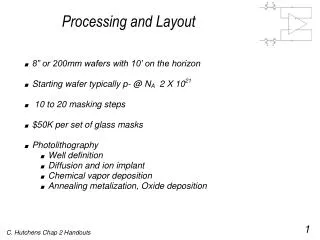
DESIGN RULES • Mask # Mask Layer Function • 1 nwell Tub for PMOS Transistor • 2 active Define Transistor D-S-ch. • 3 poly Define Transistor W & L • 4 select Threshold adjust • 5 poly contact Physical to gate by m1 • 6 active contact Physical to S & D by m1 • 7 metal 1 global interconnect • 8 via physical connect of m1 & m2 • 9 pad opening for bond wire • 10 poly2 Caps and interconnect