Download
1 / 47
470 likes | 484 Views
CMPS 255 Computer Architecture Designing a MIPS single cycle datapath PH 4.1-4.4, B, D. Review: 4-bit Ripple-Carry Binary Adder. A four-bit Ripple Carry Adder made from four 1-bit Full Adders:. 2’s Complement Adder/Subtractor. Subtraction can be done by addition of the 2's Complement.

E N D
CMPS 255Computer ArchitectureDesigning a MIPS single cycle datapath PH 4.1-4.4, B, D
Review: 4-bit Ripple-Carry Binary Adder • A four-bit Ripple Carry Adder made from four 1-bit Full Adders:
2’s Complement Adder/Subtractor • Subtraction can be done by addition of the 2's Complement. • Complement each bit. • Add 1 to the result. • The circuit shown computes A + B and A – B: • For S = 1, subtract,the 2’s complementof B is formed by usingXORs to form the 1’scomp and adding the 1applied to C0. • For S = 0, add, B ispassed throughunchanged
Overflow Detection • Overflow occurs if n + 1 bits are required to contain the result from an n-bit addition or subtraction. • Adding two unsigned numbers: overflow can be detected from the end carry out of the most significant position. • With signed number an overflow can occur for: • Addition of two operands with the same sign • Subtraction of operands with different signs • Detection can be performed by observing the carry into the sign bit (Cn -1) and the carry out of the sign bit position (Cn). If these two carries are not equal, an overflow has occurred. • Simplest way to implement overflow V = Cn + Cn-1
Clever subtractor/adder with overflow detection • N 1-bit adders 1 N-bit adder CarryIn • Symbol for 32 bit adder A 32 Sum Adder 32 B CarryOut 32
Arithmetic and Logic Unit (ALU) • Most processors contain a special logic block called ALU • easy and simple ALU does ADD, SUB, bitwise AND, bitwise OR • Symbol for 32 bit ALU OP A 32 Result ALU 32 S represents the operation B 32
Symbol 0 A C 1 B S 32-bit wide multiplexor • 32-bit wide multiplexor is an array of 32 1-bit wide multiplexor Select A 32 Y MUX 32 B 32 • 1-bit wide multiplexor • S = 0 => C = A • S = 1 => C = B
Major components of any Computer Keyboard, Mouse Memory (programs, data) Computer Devices Processor Disk(where programs, data live when not running) Input Control (“brain”) Output Datapath (“brawn”) Display, Printer 8
Fetch PC = PC+4 Exec Decode The Processor: Datapath & Control • Simplified implementation of MIPS contain only: • memory-reference instructions: lw, sw • arithmetic-logical instructions: add, sub, and, or, slt. • control flow instructions: beq, j • Generic implementation: • use the program counter (PC) to supply the instruction address and fetch the instruction from memory (and update the PC) • decode the instruction (and read registers) • execute the instruction 9
Register File 5 5 5 32 32 32 src1 addr src1 data src2 addr 32 locations dst addr src2 data write data 32 bits MIPS Register File: review • The 32 general-purpose registers are stored in register file. • Any register can be read or written by specifying its number in the file. • Four input ports: three for register numbers and one for data • Two output ports: both for data • To read a data word from the register file, we need an input port to specify the register number and an output port to carry the value that has been read • To write a data word to the register file, we need an input port to specify the register number to write to and an input port to supply the data to be written into the register 25 =
Instruction Execution • For every instruction, firsttwo steps are identical: • Send PC to memory that contains the code to fetch the instruction. • Depending on instruction type, read one or two registers: • For most instructions, read two register operands • For loadword instruction, read only one register • Subsequent actions required depend on instruction class • For all instructions, except j-type, use ALU after reading the registers. • Use ALU to calculate the actions required, for example: • memory-reference instructions use ALU for an address calculation • arithmetic-logical instructions for the operation execution • branches for comparison • After using the ALU, • load / store need to access memory either to reador write data. • arithmetic-logicalor load instruction must write data from the ALU or memory back into a register. • Lastly, based on comparison we might change next instruction address; otherwise, PC should be incremented by 4
High-level view of a MIPS implementation • Observation 1: • value written into PC can come from one of two adders, • data written into register file can come from either ALU or memory, • second input to ALU can come from register or instruction immediate field • Can’t just join wires together but multiplexorscanchoose from among multiple sources. • Observation 2: • data memory must read on a load and written on a store, • register file must be written only on a load or an arithmetic-logical instruction, • ALU must perform one of several operations • Use Control lines set on basis of various fields in the instruction direct these operations
simple datapath with the control unit and signals Control signals: used for multiplexor selection or directing the operation of a functional unit; Asserted signal : a signal is logically high (i.e., 1) Deasserted signal: a signal is logically low (i.e., 0)
rising (positive) edge Clocking Methodologies • Clocking methodology defines when signals can be read and when they can be written • if a signal is written at the same time it is read, the value of the read cannot be predictable (it could be the old value, the newly written value, or mix of both) • edge-triggered clocking methodology: means that any values stored in a sequential logic element are updated only on a clock edge • If a state element is not updated on every clock, then an explicit write control signal is required either for multiplexor selection or for directing the operation of a functional unit; 16
Clocking Methodologies • Control signal: signal used for multiplexor selection or for directing the operation of a functional unit; • data signal: contains information that is operated on by a functional unit • Edge-triggered methodology allows in the same clock cycle to: • readthe contents of a register, • send value through combinational logic, • and write that register. • Longest delay determines clock period • the logic in right figure works correctly 17
Fetch PC = PC+4 Exec Decode Fetching Instructions • Fetching instructions involves • reading the instruction from the instruction memory • updating the PC value to be the address of the next (sequential) instruction clock Increment by 4 for next instruction 32-bit register • PC is updated every clock cycle, so it does not need an explicit write control signal just a clock signal • Reading from instruction memory is a combinational activity, so it doesn’t need an explicit read control signal 18
Fetch PC = PC+4 Exec Decode Read Addr 1 Read Data 1 Register File Read Addr 2 Write Addr Read Data 2 Write Data Decoding Instructions • Decoding instructions involves • Sending the fetched instruction’s opcode and function field bits to the control unit • reading one or two values (register contents) from the Register File • Register File addresses are contained in the instruction. Control Unit Instruction 19
31 25 20 15 10 5 0 R-type: op rs rt rd shamt funct Fetch PC = PC+4 Exec Decode Executing R Format Operations • R format operations (add, sub, slt, and, or) • perform operation (opand funct) on values in rsand rt • store the result back into the Register File (into location rd) RegWrite ALU control Read Addr 1 Read Data 1 Register File Read Addr 2 overflow Instruction zero ALU Write Addr Read Data 2 Write Data • Note that Register File is not written every cycle (e.g. sw), so we need an explicit write control signal for the Register File 20
RegWrite ALU control MemWrite overflow 31 25 20 15 0 zero Read Addr 1 I-Type: Read Data 1 address offset Address op rs rt Register File Read Addr 2 Instruction Data Memory Read Data ALU Write Addr Read Data 2 Write Data Write Data MemRead Sign Extend 16 32 Executing Load and Store Operations • Load / store have to • compute a memory address: add base register (rs) to 16-bit signed offset • base register was read from the Register File during decode • sign extend offset value to create a 32-bit signed value • store value, read from register file during decode, write to data memory • load value, read from the Data Memory, must be stored in the Register File 21
31 25 20 15 0 I-Type: address offset op rs rt Executing Branch Operations • Read rs and rt then compare them for equality (zero ALU output) • Compute the branch target : add updated PC to the offset after sign extending to 32-bits and shifting left it 2 bits to turn it into a word address Branch target = [PC] + 4 + 4×offset Branch target address Add Add 4 Shift left 2 ALU control zero (to branch control logic) Read Addr 1 Instruction Memory Read Data 1 Register File Read Addr 2 PC Read Address Instruction ALU Write Addr Read Data 2 Write Data Sign Extend 16 32 22
Creating a Single Datapath from the Parts • Assemble the datapath elements, add control lines as needed, and design the controlpath • Fetch, decode and execute each instructions in one clock cycle – single cycle design • no datapath resource can be used more than once per instruction, so some resources must be duplicated (e.g., why we have a separate Instruction Memory and Data Memory) • to share datapath elements between two different instruction classes will need multiplexors at the input of the shared elements with control lines to do the selection • Cycle time is determined by length of the longest path 23
Fetch, R, and Memory Access Portions Add RegWrite ALU control MemWrite 4 ovf zero Read Addr 1 Instruction Memory Read Data 1 Address Register File Read Addr 2 Data Memory Read Address PC Instruction Read Data ALU Write Addr Read Data 2 Write Data Write Data MemRead Sign Extend 16 32 24
Add RegWrite ALUSrc ALU control MemWrite MemtoReg 4 ovf zero Read Addr 1 Instruction Memory Read Data 1 Address Register File Read Addr 2 Data Memory Read Address PC Instruction Read Data ALU Write Addr Read Data 2 Write Data Write Data MemRead Sign Extend 16 32 Multiplexor Insertion 25
System Clock MemtoReg RegWrite MemWrite Add ALUSrc ALU control 4 ovf zero Read Addr 1 Instruction Memory Read Data 1 Address Register File Read Addr 2 Data Memory Read Address PC Instruction Read Data ALU Write Addr Read Data 2 Write Data Write Data MemRead Sign Extend 16 32 Clock Distribution clock cycle 26
Add Add 4 Shift left 2 PCSrc RegWrite ALUSrc ALU control MemWrite MemtoReg ovf zero Read Addr 1 Instruction Memory Read Data 1 Address Register File Read Addr 2 Data Memory Read Address PC Instruction Read Data ALU Write Addr Read Data 2 Write Data Write Data MemRead Sign Extend 16 32 Adding the Branch Portion 27
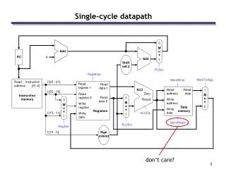
RegDst RegWrite Read Data 1 Register File 0 Read Data 2 1 Sign Extend ALU control 16 32 Instr[5-0] ALUOp (Almost) Complete Single Cycle Datapath 0 Add Add 1 4 Shift left 2 PCSrc ALUSrc MemWrite MemtoReg ovf zero Instr[25-21] Read Addr 1 Instruction Memory Address Instr[20-16] Read Addr 2 Data Memory Read Address PC Instr[31-0] Read Data 1 ALU Write Addr 0 Instr[15 -11] Write Data 0 Write Data 1 Instr[15-0] MemRead 28
Complete Datapath with Control Unit (See Next) 0 Add Add 1 4 Shift left 2 PCSrc ALUOp Branch MemRead Instr[31-26] Control Unit MemtoReg MemWrite ALUSrc RegWrite RegDst ovf Instr[25-21] Read Addr 1 Instruction Memory Read Data 1 Address Register File Instr[20-16] zero Read Addr 2 Data Memory Read Address PC Instr[31-0] 0 Read Data 1 ALU Write Addr Read Data 2 0 1 Write Data 0 Instr[15 -11] Write Data 1 Instr[15-0] Sign Extend ALU control 16 32 Instr[5-0] 29
ALU Control Unit • Controlling the ALU uses multiple decoding levels • Main control unit (seen next slides) generates the ALUOp bits • ALUOp indicates operation to be performed : add (00) for loads and stores, subtract (01) for beq, or determined by funct field (10) • For Load/StoreALU function is add to compute the memory address, for branch equal ALU function is subtract, for R-type, function depends on 6-bit funct field • ALU control unit generates ALUcontrol bits • ALU control bits based on the 2-bit ALUOp control and the 6-bit function code Notice when ALUOp code is 00 or 01, ALU action does not depend on the function field; we “don’t care” about the value of the function code, and the funct field is shown as XXXXXX. 30
ALU control truth table • Full truth table is very large (28 = 256 entries): • we don’t care about the value of the ALU control for many input combinations • X: don’t-care term indicating that output does not depend on the value of input • example, when ALUOp = 00, we always set the ALU control to 0010, independent of the function code • Once truth table has been constructed, it can be optimized and then turned into gates. 31
0 4 35 or 43 rs rs rs rt rt rt rd address address shamt funct 31:26 31:26 31:26 25:21 25:21 25:21 20:16 20:16 20:16 15:11 10:6 15:0 15:0 5:0 Main Control Unit - Control signals • Control signals derived from instruction based on following observations: • Opcodeis always in bits 31:26 • Read registers rs and rt are at positions 25:21 and 20:16 (R-type, Branch, Store) • For load and store instructions rs is the base register (25:21) • branch equal, load, and store 16-bit offset for is always at 15:0 • Destination register: rt(20:16) for a load, rd (15:11) for R- Type • add a multiplexor to select the register to be written R-type Load/Store Branch opcode always read read, except for load write for R-type and load sign-extend and add 33
Main Control Unit Truth Table • Setting of control lines depends only on opcode. Therefore, input is the 6-bit opcode field, Op [5:0] • Outputs are the control lines. • Truth table for each of the outputs based on the binary encoding of the opcodes 35
Main Control unit- Truth Table and Gates Output Input R-type Lw Sw Beq 36
(Almost) Complete Datapath with Control Unit 0 Add Add 1 4 Shift left 2 PCSrc ALUOp Branch MemRead Instr[31-26] Control Unit MemtoReg MemWrite ALUSrc RegWrite RegDst ovf Instr[25-21] Read Addr 1 Instruction Memory Read Data 1 Address Register File Instr[20-16] zero Read Addr 2 Data Memory Read Address PC Instr[31-0] 0 Read Data 1 ALU Write Addr Read Data 2 0 1 Write Data 0 Instr[15 -11] Write Data 1 Instr[15-0] Sign Extend ALU control 16 32 Instr[5-0] 37
R-type Instruction Data/Control Flow 0 Add Add 1 4 Shift left 2 PCSrc ALUOp Branch MemRead Instr[31-26] Control Unit MemtoReg MemWrite ALUSrc RegWrite RegDst ovf Instr[25-21] Read Addr 1 Instruction Memory Read Data 1 Address Register File Instr[20-16] zero Read Addr 2 Data Memory Read Address PC Instr[31-0] 0 Read Data 1 ALU Write Addr Read Data 2 0 1 Write Data 0 Instr[15 -11] Write Data 1 Instr[15-0] Sign Extend ALU control 16 32 Instr[5-0] 38
Store Word Instruction Data/Control Flow 0 Add Add 1 4 Shift left 2 PCSrc ALUOp Branch MemRead Instr[31-26] Control Unit MemtoReg MemWrite ALUSrc RegWrite RegDst ovf Instr[25-21] Read Addr 1 Instruction Memory Read Data 1 Address Register File Instr[20-16] zero Read Addr 2 Data Memory Read Address PC Instr[31-0] 0 Read Data 1 ALU Write Addr Read Data 2 0 1 Write Data 0 Instr[15 -11] Write Data 1 Instr[15-0] Sign Extend ALU control 16 32 Instr[5-0]
Load Word Instruction Data/Control Flow 0 Add Add 1 4 Shift left 2 PCSrc ALUOp Branch MemRead Instr[31-26] Control Unit MemtoReg MemWrite ALUSrc RegWrite RegDst ovf Instr[25-21] Read Addr 1 Instruction Memory Read Data 1 Address Register File Instr[20-16] zero Read Addr 2 Data Memory Read Address PC Instr[31-0] 0 Read Data 1 ALU Write Addr Read Data 2 0 1 Write Data 0 Instr[15 -11] Write Data 1 Instr[15-0] Sign Extend ALU control 16 32 Instr[5-0] 40
Branch Instruction Data/Control Flow 0 Add Add 1 4 Shift left 2 PCSrc ALUOp Branch MemRead Instr[31-26] Control Unit MemtoReg MemWrite ALUSrc RegWrite RegDst ovf Instr[25-21] Read Addr 1 Instruction Memory Read Data 1 Address Register File Instr[20-16] zero Read Addr 2 Data Memory Read Address PC Instr[31-0] 0 Read Data 1 ALU Write Addr Read Data 2 0 1 Write Data 0 Instr[15 -11] Write Data 1 Instr[15-0] Sign Extend ALU control 16 32 Instr[5-0] 41
Handling Jump Operations • Jump operation have to • replace the lower 28 bits of the PC with the lower 26 bits of the fetched instruction shifted left by 2 bits 31 0 J-Type: op jump target address Add 4 4 Jump address Instruction Memory Shift left 2 28 Read Address PC Instruction 26 42
Adding the Jump Operation Instr[25-0] 1 Shift left 2 28 32 26 0 PC+4[31-28] 0 Add Add 1 4 Shift left 2 PCSrc Jump ALUOp Branch MemRead Instr[31-26] Control Unit MemtoReg MemWrite ALUSrc RegWrite RegDst ovf Instr[25-21] Read Addr 1 Instruction Memory Read Data 1 Address Register File Instr[20-16] zero Read Addr 2 Data Memory Read Address PC Instr[31-0] 0 Read Data 1 ALU Write Addr Read Data 2 0 1 Write Data 0 Instr[15 -11] Write Data 1 Instr[15-0] Sign Extend ALU control 16 32 Instr[5-0] 44
Single Cycle Implementation Cycle Time • Unfortunately, though simple, the single cycle approach is not used because it is very slow • Clock cycle must have the same length for every instruction • What is the longest (slowest) path (slowest instruction)? 46
Instruction Critical Paths • Calculate cycle time assuming negligible delays (for muxes, control unit, sign extend, PC access, shift left 2, wires, setup and hold times) except: • Instruction and Data Memory (4 ns) • ALU and adders (2 ns) • Register File access (reads or writes) (1 ns) 47
Cycle 1 Cycle 2 Clk lw sw Waste Single Cycle Disadvantages & Advantages • Uses the clock cycle inefficiently – the clock cycle must be timed to accommodate the slowest instr • especially problematic for more complex instructions like floating point multiply • May be wasteful of area since some functional units (e.g., adders) must be duplicated since they can not be shared during a clock cycle • But it is simple and easy to understand