Prototype FPGA Tile for Subthreshold-Optimized CMOS for Ultra-Low Power Applications
This work presents a prototype FPGA tile designed for subthreshold-optimized CMOS applications, targeting ultra-low power systems. By leveraging the advantages of FPGAs, including improved energy efficiency and reconfigurability, this approach significantly enhances performance compared to traditional microcontrollers while remaining cost-effective versus ASIC solutions. The prototype's state-of-the-art low power consumption is ideal for applications such as wireless sensor networks, RFID, and digital hearing aids, achieving peak energy efficiency at sub-mW power budgets. Funded by MIT Lincoln Laboratory and the US Government.

Prototype FPGA Tile for Subthreshold-Optimized CMOS for Ultra-Low Power Applications
E N D
Presentation Transcript
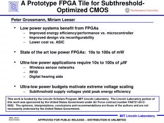
A Prototype FPGA Tile for Subthreshold-Optimized CMOS Peter Grossmann, Miriam Leeser • Low power systems benefit from FPGAs • Improved energy efficiency/performance vs. microcontroller • Improved design via reconfigurability • Lower cost vs. ASIC • State of the art low power FPGAs: 10s to 100s of mW • Ultra-low power applications require 10s to 100s of µW • Wireless sensor networks • RFID • Digital hearing aids • Ultra-low power budgets motivate extreme voltage scaling • Subthreshold supply voltages yield peak energy efficiency This work is funded by the Lincoln Scholars Program, MIT Lincoln Laboratory. The Lincoln Laboratory portion of this work was sponsored by the United States Government under Air Force contract number FA8721-05-C-0002. The opinions, interpretations, conclusions and recommendations are those of the authors and are not necessarily endorsed by the United States Government.
Prototype Tile Architecture • 2-input CLB • 4 routing channels • 32 programming bits • Flexible I/O
Prototype Tile Demonstration • Functional verification of all tile components through implementation of serial adder • Tile average power ≈ tens of nanowatts • Enables useful circuits on sub-mW power budgets • Implementation of 6x6 tile array on test chip currently in fabrication at Lincoln Laboratory Serial Adder