Download
1 / 35
350 likes | 433 Views
This thesis defense outlines using CMOS technology for DNA detection, focusing on design details, experimental results, and concluding with future work. The microarray scanner design aims to be integrated, reduce cooling costs, and validate without cooling, featuring an Active Pixel Sensor with a ΔΣ Modulator for photon-to-electron conversion and signal capture. Experimental results show limitations in dark signal and light sensitivity, aiming to enhance sensitivity, conversion gain, reduce noise, and improve optical coupling for accurate DNA detection.

E N D
A CMOS Imager for DNA Detection Samir Parikh MASc Thesis Defense Dept. of Electrical and Computer Engineering University of Toronto 24th January, 2007
Outline • Introduction • Motivation and Objectives • Design Details • Experimental Results • Conclusion • Future Work
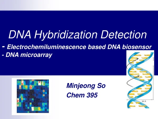
Introduction: DNA Microarrays • DNA microarrays used to detect DNA sequence concentration Chemical Processing DNA ssDNA Fragments • DNA is split into its two constituent strands • One strand is broken into fragments
Introduction: Using DNA Microarrays • Within a spot multiple identical ssDNA probes are attached • Each spot is tailored to match with a particular target ssDNA sequence • target ssDNA is created from Messenger RNA extracted from a cell
Introduction: DNA Detection • Solution containing target ssDNA+fluorescing dye molecule is introduced to the slide • Spots on the DNA microarray pair/unpair depending on the nucleotide sequence of the probe and target ssDNA • DNA microarray is washed to remove unpaired target ssDNA
Introduction: DNA Detection • Solution containing target ssDNA+fluorescing dye molecule is introduced to the slide • Spots on the DNA microarray pair/unpair depending on the nucleotide sequence of the probe and target ssDNA • DNA microarray is washed to remove unpaired target ssDNA
Introduction: Basic Microarray Scanner • Fluorescing dye molecule absorbs energy at λ1nm and emits energy at λ2nm • Light detectors are discussed in the next slide
Introduction: Existing Light Detectors • Commonly used detectors in microarray scanners are: • Photomultiplier Tube (PMT) - accurate • Charge-Coupled Device (CCD) - fast
Motivation and Objectives • Determine the feasibility of using standard CMOS technology for light detection and quantification • Integrated • Smaller • Cheaper • Validate the design without the use of cooling • Reduce cost related to cooling • Reduce power consumption due to cooling equip.
Design Details: Microarray Scanner • Signal from entire spot captured at once
Design Details: Microarray Scanner • Signal from entire spot captured at once
Design Details: Microarray Scanner • Signal from entire spot captured at once
Design Details: Microarray Scanner • Signal from entire spot captured at once
Design Details: Microarray Scanner • Signal from entire spot captured at once
Design Details: Active Pixel Sensor (APS) • 5-transistor circuit with pseudo-differential output • Pinned photodiode performs the photon-to-electron conversion • Circuits has two phases: reset and integration photons
Design Details: ΔΣ Modulator • 2nd Order Discrete-Time ΔΣ • Can be combined with a decimation filter for a complete ADC • Boser-Wooley Architecture • Delaying Integrators with 1bit feedback • Folded-Cascode Op-amp used
Experimental Results: APS • Dark signal limits the integration time for the APS • Low light sensitivity sets the min # of photons detectable
Experimental Results: ΔΣ Modulator • Simulation includes flicker and thermal noise • Close matching between simulation and measured
Experimental Results: ΔΣ Modulator • Commercial microarray scanners have 12 to 16-bits accuracy • Sampling rate sets an upper limit on the maximum light level • Sampling rate not critical, minimum light level is more important
Experimental Results: Scanner Characterization Slide • Slide contains spots with dilution series • Each spot contains fluorescing dye molecules with fixed density • Spot density (fluorophores/um2) decreases at a fixed rate Decreasing dye density
Discussion: Microarray Scanner • Portability Potential • Microarray scanner: Smaller, integrated detector w/o cooling • Agilent scanner: PMT • Detection Limit • Microarray scanner: 4590 fluorophores/um2 • Agilent scanner: 4 fluorophores/um2 • Resolution and Scan time • Microarray scanner: Larger pixel→Entire spot imaged at once • Agilent scanner: 10μm resolution→takes longer to image a spot • Microarray scanner: Multiple pixels → short scan time • Agilent scanner: Single element → long scan time (8 min/slide)
Discussion: APS • Dark signal of APS not the limiting factor • Background of the slide = 1.5 ADU/sample • Dark signal of the APS = 0.08 ADU/sample • Integration time of the APS is limited by the slide background • Improve the sensitivity of the APS beyond 2.6х10-2 lux • Increase its conversion gain • Reduce its read noise and reset noise
Discussion:Optical and Mechanical • Improve optical coupling between APS ↔ fluorescing spots • Use a focusing/collimating element • Compensate for slide tilt • Reduce laser noise and drift from 3% to 0.1% • Improved power supply • Better laser control/feedback
Conclusion • Standard CMOS technology shows potential to be an alternative to existing PMT/CCD detectors used in microarray scanners • The detection limit of a microarray scanner is determined by: • Mechanical and Optical Non-idealities • Detector Non-idealities
Future Work • Improve the conversion gain of the APS • Reduce the read noise, and reset noise of the APS • Improve the accuracy of the ADC