Download
1 / 48
480 likes | 536 Views
Explore the transition from discrete devices to sophisticated FPGA technology incorporating various programmable logic methods. Learn about gate arrays, PALs, PLAs, and tradeoffs in FPGA design and implementation.

E N D
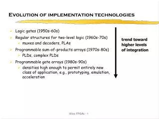
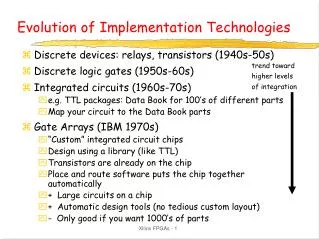
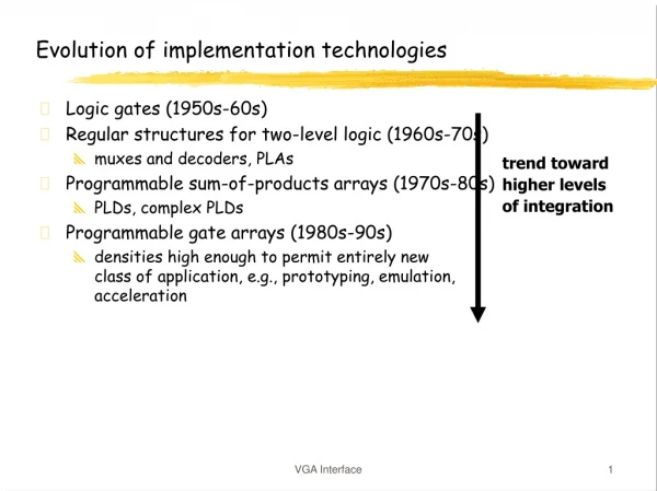
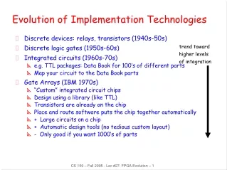
Evolution of Implementation Technologies • Discrete devices: relays, transistors (1940s-50s) • Discrete logic gates (1950s-60s) • Integrated circuits (1960s-70s) • e.g. TTL packages: Data Book for 100’s of different parts • Map your circuit to the Data Book parts • Gate Arrays (IBM 1970s) • “Custom” integrated circuit chips • Design using a library (like TTL) • Transistors are already on the chip • Place and route software puts the chip together automatically • + Large circuits on a chip • + Automatic design tools (no tedious custom layout) • - Only good if you want 1000’s of parts trend toward higher levels of integration CS 150 – Fall 2005 - Lec #27: FPGA Evolution – 1
Gate Array Technology (IBM - 1970s) • Simple logic gates • Use transistors toimplement combinationaland sequential logic • Interconnect • Wires to connect inputs andoutputs to logic blocks • I/O blocks • Special blocks at peripheryfor external connections • Add wires to make connections • Done when chip is fabed • “mask-programmable” • Construct any circuit CS 150 – Fall 2005 - Lec #27: FPGA Evolution – 2
Programmable Logic • Disadvantages of the Data Book method • Constrained to parts in the Data Book • Parts are necessarily small and standard • Need to stock many different parts • Programmable logic • Use a single chip (or a small number of chips) • Program it for the circuit you want • No reason for the circuit to be small CS 150 – Fall 2005 - Lec #27: FPGA Evolution – 3
Programmable Logic Technologies • Fuse and anti-fuse • Fuse makes or breaks link between two wires • Typical connections are 50-300 ohm • One-time programmable (testing before programming?) • Very high density • EPROM and EEPROM • High power consumption • Typical connections are 2K-4K ohm • Fairly high density • RAM-based • Memory bit controls a switch that connects/disconnects two wires • Typical connections are .5K-1K ohm • Can be programmed and re-programmed in the circuit • Low density CS 150 – Fall 2005 - Lec #27: FPGA Evolution – 4
Programmable Logic • Program a connection • Connect two wires • Set a bit to 0 or 1 • Regular structures for two-level logic (1960s-70s) • All rely on two-level logic minimization • PROM connections - permanent • EPROM connections - erase with UV light • EEPROM connections - erase electrically • PROMs • Program connections in the _____________ plane • PLAs • Program the connections in the ____________ plane • PALs • Program the connections in the ____________ plane CS 150 – Fall 2005 - Lec #27: FPGA Evolution – 5
PAL Logic Building Block • Programmable AND gates • Fixed OR/NOR gate • Flipflop/Registered Output • Feedback to Array • Tri-state Output CS 150 – Fall 2005 - Lec #27: FPGA Evolution – 6
XOR PALs • Useful for comparator logic, arithmetic sums, etc. • Use of XOR gates can dramatically reduce the number of AND plane inputs needed to realize certain functions CS 150 – Fall 2005 - Lec #27: FPGA Evolution – 7
XOR PAL • And/Or/XOR Logic • Feedback • Registered Outputs • Tri-State Outputs CS 150 – Fall 2005 - Lec #27: FPGA Evolution – 8
CLK Q0 Seq N Q1 Seq D D D D Q Q Q Open Com Reset Another Variation: Synchronous vs. Asynchronous Outputs CS 150 – Fall 2005 - Lec #27: FPGA Evolution – 9
Making Large Programmable Logic Circuits • Alternative 1 : “CPLD” • Put a lot of PLDS on a chip • Add wires between them whose connections can be programmed • Use fuse/EEPROM technology • Alternative 2: “FPGA” • Emulate gate array technology • Hence Field Programmable Gate Array • You need: • A way to implement logic gates • A way to connect them together CS 150 – Fall 2005 - Lec #27: FPGA Evolution – 10
Field-Programmable Gate Arrays • PALs, PLAs = 10s – 100s Gate Equivalents • Field Programmable Gate Arrays = FPGAs • Altera MAX Family • Actel Programmable Gate Array • Xilinx Logical Cell Array • 1000s - 100000(s) of Gate Equivalents! CS 150 – Fall 2005 - Lec #27: FPGA Evolution – 11
Field-Programmable Gate Arrays • Logic blocks • To implement combinationaland sequential logic • Interconnect • Wires to connect inputs andoutputs to logic blocks • I/O blocks • Special logic blocks at periphery of device forexternal connections • Key questions: • How to make logic blocks programmable? • How to connect the wires? • After the chip has been fabbed CS 150 – Fall 2005 - Lec #27: FPGA Evolution – 12
Tradeoffs in FPGAs • Logic block - how are functions implemented: fixed functions (manipulate inputs) or programmable? • Support complex functions, need fewer blocks, but they are bigger so less of them on chip • Support simple functions, need more blocks, but they are smaller so more of them on chip • Interconnect • How are logic blocks arranged? • How many wires will be needed between them? • Are wires evenly distributed across chip? • Programmability slows wires down – are some wires specialized to long distances? • How many inputs/outputs must be routed to/from each logic block? • What utilization are we willing to accept? 50%? 20%? 90%? CS 150 – Fall 2005 - Lec #27: FPGA Evolution – 13
Altera EPLD (Erasable Programmable Logic Devices) • Historical Perspective • PALs: same technology as programmed once bipolar PROM • EPLDs: CMOS erasable programmable ROM (EPROM) erased by UV light • Altera building block = MACROCELL 8 Product Term AND-OR Array + Programmable MUX's I/O Pin Seq. Logic Block Programmable polarity Programmable feedback CS 150 – Fall 2005 - Lec #27: FPGA Evolution – 14
Altera EPLD: Synchronous vs. Asynchronous Mode Altera EPLDs contain 10s-100s of independently programmed macrocells Personalized by EPROM bits: Flipflop controlled by global clock signal local signal computes output enable Flipflop controlled by locally generated clock signal + Seq Logic: could be D, T positive or negative edge triggered + product term to implement clear function CS 150 – Fall 2005 - Lec #27: FPGA Evolution – 15
Altera Multiple Array Matrix (MAX) AND-OR structures are relatively limited Cannot share signals/product terms among macrocells Logic Array Blocks (similar to macrocells) Global Routing: Programmable Interconnect Array EPM5128: 8 Fixed Inputs 52 I/O Pins 8 LABs 16 Macrocells/LAB 32 Expanders/LAB CS 150 – Fall 2005 - Lec #27: FPGA Evolution – 16
LAB Architecture I/O Pad Macrocell I/O ARRAY Block I I/O Pad N P P I U A T Expander S Product Term ARRAY • Expander Terms shared among all • macrocells within the LAB • Efficient way to use AND plane resources CS 150 – Fall 2005 - Lec #27: FPGA Evolution – 17
P22V10 PAL Supports large number of product terms per output Latches and muxes associated with output pins CS 150 – Fall 2005 - Lec #27: FPGA Evolution – 18
Actel Programmable Gate Arrays Rows of programmable logic building blocks + rows of interconnect Anti-fuse Technology: Program Once Use Anti-fuses to build up long wiring runs from short segments 8 input, single output combinational logic blocks FFs constructed from discrete cross coupled gates CS 150 – Fall 2005 - Lec #27: FPGA Evolution – 19
Actel Logic Module Basic Module is a Modified 4:1 Multiplexer Example: Implementation of S-R Latch CS 150 – Fall 2005 - Lec #27: FPGA Evolution – 20
Actel Interconnect Interconnection Fabric CS 150 – Fall 2005 - Lec #27: FPGA Evolution – 21
Actel Routing Example Jogs cross an anti-fuse minimize the # of jogs for speed critical circuits 2 - 3 hops for most interconnections CS 150 – Fall 2005 - Lec #27: FPGA Evolution – 22
Actel’s Next Generation: Axcelerator • C-Cell • Basic multiplexer logic plus more inputs and support for fast carry calculation • Carry connections are “direct” and do not require propagation through the programmable interconnect CS 150 – Fall 2005 - Lec #27: FPGA Evolution – 23
R-Cell Core is D flip-flop Muxes for altering the clock and selecting an input Feed back path for current value of the flip-flop for simple hold Direct connection from one C-cell output of logic module to an R-cell input; Eliminates need to use the programmable interconnect Interconnection Fabric Partitioned wires Special long wires Actel’s Next Generation: Accelerator CS 150 – Fall 2005 - Lec #27: FPGA Evolution – 24
Xilinx Programmable Gate Arrays • CLB - Configurable Logic Block • 5-input, 1 output function • or 2 4-input, 1 output functions • optional register on outputs • Built-in fast carry logic • Can be used as memory • Three types of routing • direct • general-purpose • long lines of various lengths • RAM-programmable • can be reconfigured CS 150 – Fall 2005 - Lec #27: FPGA Evolution – 25
Programmable Interconnect I/O Blocks (IOBs) Configurable Logic Blocks (CLBs)
The Xilinx 4000 CLB CS 150 – Fall 2005 - Lec #27: FPGA Evolution – 27
Two 4-input functions, registered output CS 150 – Fall 2005 - Lec #27: FPGA Evolution – 28
5-input function, combinational output CS 150 – Fall 2005 - Lec #27: FPGA Evolution – 29
CLB Used as RAM CS 150 – Fall 2005 - Lec #27: FPGA Evolution – 30
Fast Carry Logic CS 150 – Fall 2005 - Lec #27: FPGA Evolution – 31
Xilinx 4000 Interconnect CS 150 – Fall 2005 - Lec #27: FPGA Evolution – 32
Switch Matrix CS 150 – Fall 2005 - Lec #27: FPGA Evolution – 33
Xilinx 4000 Interconnect Details CS 150 – Fall 2005 - Lec #27: FPGA Evolution – 34
Global Signals - Clock, Reset, Control CS 150 – Fall 2005 - Lec #27: FPGA Evolution – 35
Xilinx 4000 IOB CS 150 – Fall 2005 - Lec #27: FPGA Evolution – 36
Xilinx FPGA Combinational Logic Examples • Key: General functions are limited to 5 inputs • (4 even better - 1/2 CLB) • No limitation on function complexity • Example • 2-bit comparator: A B = C D and A B > C D implemented with 1 CLB(GT) F = A C' + A B D' + B C' D' (EQ) G = A'B'C'D'+ A'B C'D + A B'C D'+ A B C D • Can implement some functions of > 5 input CS 150 – Fall 2005 - Lec #27: FPGA Evolution – 37
Xilinx FPGA Combinational Logic • Examples • N-input majority function: 1 whenever n/2 or more inputs are 1 • N-input parity functions: 5 input/1 CLB; 2 levels yield 25 inputs! 5-input Majority Circuit 9 Input Parity Logic CLB CLB 7-input Majority Circuit CLB CLB CLB CLB CS 150 – Fall 2005 - Lec #27: FPGA Evolution – 38
Xilinx FPGA Adder Example • Example • 2-bit binary adder - inputs: A1, A0, B1, B0, CIN outputs: S0, S1, Cout Full Adder, 4 CLB delays to final carry out 2 x Two-bit Adders (3 CLBs each) yields 2 CLBs to final carry out CS 150 – Fall 2005 - Lec #27: FPGA Evolution – 39
Xilinx Vertex-II Family • 88-1000+ pins • 64-10000+ CLBs • Combinational and sequential logic using lookup tables and flip-flops • Random-access memory • Shift registers for use as buffer storage • Multipliers regularly placed throughout the CLB array to accelerate digital signal processing applications • E.g., the XC2V8000: 11,648 CLBs, 1108 IOBs, 90,000+ FFs, 3Mbits RAM (168 x 18Kbit blocks), 168 multipliers • Equivalent to eight million two-input gates! CS 150 – Fall 2005 - Lec #27: FPGA Evolution – 40
Tri-state/bidirectional driver Registers for each of three signals involved: input, output, tri-state enable. Two registers to latch values with separate clocks. For large pinouts, separate clocks stagger signals changes to avoid large current spikes FFs used for synchronization as well as latching Xilinx Vertex-II Family IOB CS 150 – Fall 2005 - Lec #27: FPGA Evolution – 41
Four basic slices in two groups Each has a fast carry-chain Local interconnect to wire logic of each slice and connect to the CLB array: switch matrix is large collection of programmable switches Xilinx Vertex-II Family CLB CS 150 – Fall 2005 - Lec #27: FPGA Evolution – 42
Just ½ of one slice! 4-input LUT + FF Fast carry logic Many programmable interconnections for sync vs. async operation Xilinx Vertex-II Family CLB Internals CS 150 – Fall 2005 - Lec #27: FPGA Evolution – 43
A AB C B 1 (AÅB)Ci (AÅBÅCi) (AÅB) 0 Xilinx Vertex-II Family Fast Carry Logic Co 1 1 (AÅB)Ci+AB 1 1 Mux A B 0 1 LUT Mux 0 1 A B LUT Ci CS 150 – Fall 2005 - Lec #27: FPGA Evolution – 44
Sequential Portion Two positive edge-triggered flip-flops Transparent latches or flip-flops Asynchronous or synchronous sets and resets Initialize to different values at power-up Clocks and load enables complemented or not Xilinx Vertex-II Family CLB CS 150 – Fall 2005 - Lec #27: FPGA Evolution – 45
4-input function generator OR 16 bits of dual-ported random-access memory (with separate address inputs for read - G1 to G4 - and write - WG1 to WG4) OR a 16-bit variable-tap shift register With muxes, CLB can implement any function of 8 inputs and some functions of 9 inputs Registered and unregistered versions of function block outputs Xilinx Vertex-II Family Slice Personality CS 150 – Fall 2005 - Lec #27: FPGA Evolution – 46
Methods of interconnecting CLBs and IOBs: (1) direct fast connections within a CLB (2) direct-connections between adjacent CLBs (3) double-lines to fanout signals to CLBs one or two away (4) hex lines to connect to CLBs three or six away (5) long lines that span the entire chip Fast access to neighbors vertically and horizontally with direct connections Double and hex lines provide a slightly larger range Long lines saved for time-critical signals w/ min signal skew Xilinx Vertex-II Family Interconnections CS 150 – Fall 2005 - Lec #27: FPGA Evolution – 47
Programmable Logic Summary • Discrete Gates • Packaged Logic • PLAs • Ever more general architectures of programmable combinational + sequential logic and interconnect • Altera • Actel • Xilinx—4000 series to Vertex • CLBs implementing logic function generators, RAMs, Shift registers, fast carry logic • Local, inter-CLB, and long line interconnections CS 150 – Fall 2005 - Lec #27: FPGA Evolution – 48