Download
1 / 29
430 likes | 691 Views
Chemical etching effects in porous silicon layers. Daniel Navarro Urrios Dpto. de Física Básica, University of La Laguna, Spain INFM and Dipartimento di Fisica, University of Trento, Italy. Co-workers. C. Pérez-Padrón, E. Lorenzo, N. E. Capuj.

E N D
Chemical etching effects in porous silicon layers Daniel Navarro Urrios Dpto. de Física Básica, University of La Laguna, Spain INFM and Dipartimento di Fisica, University of Trento, Italy
Co-workers C. Pérez-Padrón, E. Lorenzo, N. E. Capuj Dpto. de Física Básica, University of La Laguna, Avda. Astrofísico Fco. Sánchez, La Laguna, 38071 Spain Z. Gaburro, C. J. Oton and L. Pavesi INFM and Dipartimento di Fisica, University of Trento, Via Sommarive 14, Povo, Trento 38050 Italy
Introduction and motivations Interferometric measurements PL measurements Conclusions Index
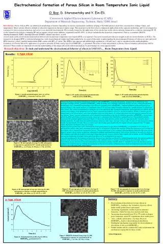
What is porous silicon? Nanostructured spongeous silicon Electrochemically etched with HF Introduction to porous silicon • Properties of PS: • Luminescent (quantum confinement) • Optically homogeneous • Modulable refractive index with current • Promising for photonics
HF chemically etches off porous silicon (porosity increases slowly) Also luminescence properties depend on porosity (Quantum confinement) Introduction HF Porous silicon formation is slightly non-homogeneous in depth I
Study the changes induced by chemical etching: - Optical (in-situ refractive index monitoring) - Structural (electronic microscopy) - Light emission (PL) Motivations
Introduction and motivations Interferometric measurements PL measurements Conclusions Index
Low light intensity! 2 l PS Experimental setup Photodetector Attenuation Filter Mirror Platinum electrode He-Ne laser HF c-Si
2 l Frequency opt. path change rate What we can see Optical path difference between the two rays During the anodization, the optical path increases
The phase changes sign! Refractive index decrease After anodization, there is still an oscillating signal!
The signal frequency is the same before and after It is an irreversible chemical process, not a transient Could the post- etching oscillations be a transient? (out-diffusion of chemical species, micro-bubbles…) Short current pulse
Signal frequency: During the post-etching we consider: - constant thickness - variations in refractive index (nPS) Frequency proportional to the sample thickness and to the refractive index change rate
Results We studied samples with different anodization times: (increasing thickness) 400 s 800 s 1200 s 1600 s
Normalizing to the thickness The index change rate is independent on thickness Results Frequency vs. post-etching time They overlap Two different exponential decays: One fast (400 s) One slow (8200 s)
2400 sec 1200 sec No post-etching 50 nm 50 nm 50 nm Beginning of the slow process Fast post etching process TEM micrographs (Sample thickness: 500 nm) Different post-etching times:
What is happening Chemical etching enlarges the pores and reduces the wall thickness
Introduction and motivations Interferometric measurements PL measurements Conclusions Index
A blueshift is expected PL measurements What happens with the PL? Porous silicon luminescence is associated with quantum confinement in the nanostructures Post-etching reduces the nanostructure size
PL measurements We studied samples with the same anodization time (400s) (same thickness) Different post-etching times 0 s 1200 s 1800 s 5200 s 12000 s 18000 s
PL measurements First minutes During post-etching, a short wavelength contribution appears, and then disappears It can be associated with the fast etching of a rough nanostructure on the walls of the pores
PL measurements Long post-etching times (waterfall plot) The main PL peak blue-shifts Walls of the pores become thinner, increasing the quantum confinement
Introduction and motivations Interferometric measurements PL measurements Conclusions Index
Conclusions • HF chemically etches porous silicon homogeneously • Increasing porosity • Decreasing refractive index • For short times: • Fast index decrease • A blue component appears and disappears • For long times: • - Slow index decrease • - Slow blue-shift of the main PL peak
Acknowledgements We acknowledge Spanish Ministry of Science and Technology Project MAT 2002-00044, the Canary Islands Government (Project No. PI2001/093, PI2001/074), the European project EC-SINERGIA and the Italian INFM project PAIS-SMOG. we thank Professors I. Martín and S. Gialanella