Download
1 / 32
1.4k likes | 4.32k Views
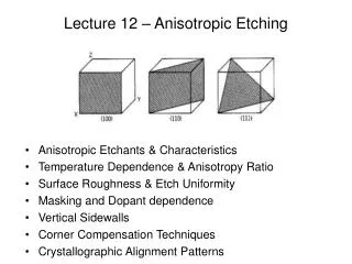
Chapter 10 Etching. Introduction to etching. Wet chemical etching: isotropic. Anisotropic etching of crystalline Si. Dry etching overview. Plasma etching mechanism. Types of plasma etch system. Dry etching issues. Dry etching method for various films.

E N D
Chapter 10 Etching • Introduction to etching. • Wet chemical etching: isotropic. • Anisotropic etching of crystalline Si. • Dry etching overview. • Plasma etching mechanism. • Types of plasma etch system. • Dry etching issues. • Dry etching method for various films. • Deep Si etching (can etch through a wafer). NE 343: Microfabrication and thin film technology Instructor: Bo Cui, ECE, University of Waterloo; http://ece.uwaterloo.ca/~bcui/ Textbook: Silicon VLSI Technology by Plummer, Deal and Griffin
Main issues in plasma etching PR: photoresist CD: critical dimension Etch profiles
Etched profile control Lateral etch of resist widens the opening gradually. Ion trajectory problem causes bowing profile
Profile control by sidewall passivation Si etched in BCl3/HCl/O2 plasma Too much passivation Micro-masking For Cl- or Br- based etching of Si, need to remove the hard-mask such as SiO2 first, before etching the Si. Here it is not completely removed.
Profile control by “substrate bias” • The bias is the self-bias in RF plasma, not applied DC voltage. • For Si, slight etch even without ion bombardment, so sidewall is always etched as well. Ideally, bias voltage increases etch rate Vz, but not Vx. • For SiO2, no (actually some) etch without ion bombardment, so always vertical sidewall (in reality, some bombardment on sidewall, thus some lateral etch).
Etch rate affected by gas pressure and loading effect Etch rate reactive species flux (neutrals and ions) J = CV C plasma density & pressure; V bias RF power Plasma density • An optimal pressure exists for maximum etching rate. • However, in reality, etching rate is not the only issue. • For example, if anisotropy is the most important factor, one should use lower pressure. • Moreover, sometimes etching rate doesn’t depend on pressure very much, because the rate is limited by chemical reaction (depends on temperature) . RF power + inductively coupled power Etching uniformity: loading effect Rate • “Bull’s eye”: wafer etches faster at outside, slower inside (e.g. Barrel etcher). • “Macro-loading”: too many wafers rob others of etchant (long-range gas transport problem). “Bull’s eye” effect is one type of macro-loading effect. • “Micro-loading”: unmasked large areas consumed too much etchant (short-range gas transport problem).
Aspect ratio and micro-loading effect • Micro-loading: etch rate depends on local pattern density. • Aspect-ratio dependent etching, RIE-lag: smaller features etch more slowly, because: • Etchants are more difficult to pass through the smaller hole. • Etch byproducts are harder to diffuse out. • Lower pressure can minimize the effect: more directional and longer mean free path, easier for etchants to reach the trench/hole bottom and for etch byproducts to get out. Micro-loading and sidewall bowing in Si etched with HSQ/AZPN114 bi-layer mask in Cl2/HBr plasma. mask silicon
When to stop etching: main etch & over etch • Film thickness and etch rate is not uniform, needs over-etch to remove possible leftover film. • Selectivity of etched film and substrate is very important. • RIE uses optical endpoint detection to switch from main etch to over etch. For R&D tool, usually no endpoint detection installed, thus often one does a lot of over-etch to make sure etching is finished. This requires high selectivity to minimize substrate etch. Start main etch Before over etch After over etch
Etching endpoint detection by optical emission spectroscopy • Each atom/molecule has its own emission wavelength. • Color of plasma changes when etch different materials • Optical sensors can be used to detect the change and indicate the endpoint for plasma etch processes. Excited state I Excited state II Ground state
Etching endpoint detection setup Etching chamber • Easy accomplished, in-situ, non-intrusive. • Spectrum 200-900 nm is usually detected. • Good sensitivity for endpoint detection. • The light emitted from plasma is sent to the mono-chromator via lens and/or optical fiber. • Mono-chromator can be replaced by Optical Multi-channel Analyzer (OMA). • Detector can be a CCD or Photo-Multiplier Tube (PMT). Endpoint detection
Chapter 10 Etching • Introduction to etching. • Wet chemical etching: isotropic. • Anisotropic etching of crystalline Si. • Dry etching overview. • Plasma etching mechanism. • Types of plasma etch system. • Dry etching issues. • Dry etching method for various films. • Deep Si etching (can etch through a wafer). NE 343: Microfabrication and Thin Film Technology Instructor: Bo Cui, ECE, University of Waterloo, bcui@uwaterloo.ca Textbook: Silicon VLSI Technology by Plummer, Deal, Griffin
Plasma etch methods for various films: overview • Most reactant gasses contain halogens: F, Cl, Br, or I • Exact choice of reactant gasses to etch each specific film depends on • Ability to form volatile by-products that can be removed by pumping • Selectivity and anisotropy. • Boiling points are good indicators of volatility of species • Lower boiling point, higher tendency to evaporate. • High boiling point may need etching at elevated temperatures.
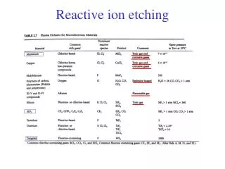
Typical or representative plasma etch gases for films used in IC fabrication Table 10-3
RIE/plasma etch gases: from another book Most lab systems have only fluorine-based gases (SF6, CF4, CHF3) since they are relatively safe; chlorine-based gases are corrosive. Most RIE has Ar and O2 gas, some has H2 and He.
Plasma etching of silicon dioxide (using CF4) • Etching is mostly done by reactive neutral species - free radicals such as F. • Additives like O2 can be used that react with CF3 (and CF2, form CO and CO2) and reduce CF3 + F recombination, thus higher F concentration and higher etch rate. • However, too much O2 reduces etch rate due to dilution effect, competition of O with F for surface sites, and reversal of the second reaction (form oxide with SiF4). • These processes are chemical (spontaneous, can etch without ion bombardment) and are therefore pretty isotropic and selective. • Nonetheless, for low pressure where ion energy is high, damage-driven ion-enhanced attack dominates, thus anisotropic etching. • The situation is similar for SF6 and NF3 gas. • The key to promote anisotropy as well as increasing selectivity over Si is to reduce F and increase C, because then: • Etching is more done by CF3 or CF2 (than by F), which is strongly ion-enhanced (appreciable etching happens only where ion bombardment occurs). • Polymer inhibitor formation is increased, which protects the sidewall. • This is realized by adding H2 that reacts with/consumes F to form HF. • Or by using fluorine-poor and carbon-rich gases such as CHF3, C3F8 and C2F6.
Effect of C/F ratio Effect of C/F ratio Inhibitor: Teflon like fluorocarbon polymer Figure 10-24. Fluorocarbon polymer • High bias voltage (400 - 500eV) can enhance vertical etch rate by removing inhibitor at bottom. • Ar+ (heavy) can also be used to remove inhibitor at pattern bottom. Because it is inert, this does not effect the chemistry of the plasma. • Reduction of F/C ratio of the etch gas improves selectivity of SiO2 over Si. • For some applications, polymer inhibitor on sidewalls needs to be removed with O2 or CF4 after etching is done.
Too low F/C ratio leads to net inhibitor deposition (kind of like PECVD) like PECVD, net film deposition rather than etching • The addition of H2 removes F from the system by forming stable HF (not very reactive) gas, which reduces F/C ratio and slows down the formation of SiF4 and thus the etching rate. • With less F, the chance of CF2,3 to combine with F to form CF4 is lower, thus higher CF2,3 concentration, which promotes the formation of fluorocarbon polymer. • Addition of H2 increases selectivity of SiO2 with respect to silicon. Because: • Increased polymerization tends to inhibit etching. However, on horizontal surfaces , ionic bombardment provides enough energy, causing the carbon/hydrogen (1-2nm F-C polymer on oxide surface) to combine with surface oxygen, releasing CO and H2O. • Once O in Si-O is gone, Si has a dangling bond, which is removed by combining with released fluorine radicals. • Silicon will not be etched (if H2 is high enough) because of the absence of oxygen at the surface. The F-C polymer on surface can be very thick (>15nm), stopping etching.
Effect of F/C ratio on selectivity between SiO2 and Si Si Net polymer deposition SiO2 Etching rate (nm/min) Etching rate (nm/min) SiO2 Si Percentage of O2 in CF4/O2 Percentage of H2 in CF4/H2 Adding O2 enhances Si etch: O2 combines with CF3, CF2 reducing their recombination with F. But too much O2 dilutes F, O competes with F for surface sites (equivalent to oxidization of Si, knowing that SiO2 etches slower than Si by F), and O2 may react with SiF4 to form SiO2. For CHF3, one F bond with H to form HF that is pumped away. So ratio is 1:2 (not 1:3).
Plasma/RIE etching of silicon • F-based chemistry (CF4, SF6, NF3) tend to be isotropic. • When anisotropy is not important, SF6/O2 is a good chemistry for high selectivity. • When anisotropy is desired, one can use CF4/H2 (or CHF3), but undercutting may still occur. • Or just use low pressure to promote ion-damage enhanced etching. • Hard to achieve using F simultaneously high anisotropy and selectivity over SiO2. • Cl-based chemistry (Cl2, HCl, SiCl4, BCl3) result in anisotropic and selective etching (yet etch rate lower than F chemistry). • Etch needs to be ion bombardment-enhanced. • Thus anisotropic without polymer inhibitor formation. • Selectivity to oxide is very high (100:1). • Anisotropy enhanced by adding small amount of O2 (form SiO2 inhibitor on sidewall, those formed on bottom bombarded away) • Br-based chemistry (HBr, Br2) are similar to chlorine based etchants (etch rate slower than F or Cl). • More anisotropic and selective to oxide than F- and Cl-based RIE without polymer inhibitor • Adding O2 promotes inhibitor formation (forming SiO2 from Si) and increase selectivity over oxide (due to removal of C from resist erosion). Effect of H2 on profile. (good book)
Chlorine Si RIE: doping is also very important • Un-doped Si etch slowly in Cl/Cl2 ambient without addition of ion bombardment. • Heavily n-type doped Si etches without bombardment in Cl, but not in Cl2. • Doping implies that Cl etching involves electron transfer from substrate. • Atomic Cl chemisorbs on Si. Once surface Cl becomes negatively charged, it can bond ionically with the substrate. This frees additional chemisorption sites and increases probability that Cl atoms penetrate surface and produce volatile silicon chlorides. • Cl penetration is increased by ion bombardment, leading to energy-driven anisotropy. • Charge transfer produces isotropic etch in heavily doped layers. Yet one can obtain anisotropic etch by sidewall polymerization. • Polymerization is done by adjusting relative concentrations of Cl2 and BCl3, CCl4 or SiCl4. Like CF4 plasma, in Cl2/CCl4 gas, etching is mainly by atom (Cl), and polymerization by molecule radial (CCl3, CCl2). ICP plasma etching of poly-Si usually consists of three steps For un-doped Si (top), once a monolayer of Cl builds on surface, it impedes any Cl addition.
Plasma/RIE etching aluminum Al etching using CCl4, (Cl2 is more popular) • Fluorine is not used because AlF3 is not volatile. • Presence of native oxide Al2O3 on Al surface requires a breakthrough etch before the main etch: Ar sputter, or use BCl3, SiCl4, CCl4 or BBr3 to scavenge O2 & H2O and remove Al2O3 by both physical and chemical means. • Cl2 etches Al isotropically (pure chemical, no need of ion bombardment for etching). • For anisotropic etching, need form sidewall inhibitor: add CHCl3, CFCl3, CCl4, BCl3 or N2 (form CN polymer from resist erosion). • Al/Cu alloys are used in interconnects but Cu does not etch in Cl. • Etch requires ion bombardment or high temperature • Corrosion of Al line occurs when exposed to ambient because Cl or AlCl3 on sidewall and resist react with water to form HCl which etches Al. • To passivate Al surface after etch before exposure to atmosphere: • Heat wafer to 100-150oC to drive-off Cl. • Bury Cl with CHF3 plasma-induced C-F polymer and remove the polymer later. • Expose to F ambient such as CF4 plasma to replace Cl with F. • Then O2 plasma to remove photoresist, followed by DI water rinse.
Photoresist(PR) stripping by oxygen plasma This is also very frequently used for surface cleaning. PR Film Si The etch product is CO, CO2 and H2O… Adding CF4, N2, H2, or H2O to oxygen plasma can increase O-atom concentration and hence the PR stripping rate. For few % addition of CF4, F takes H from chain forming HF, which makes O easier to cut chain. (O replace H and bond to C1, then C1-C2 breaks to form double bond O=C1) Etching can be anisotropic if pressure is low.
Chapter 10 Etching • Introduction to etching. • Wet chemical etching: isotropic. • Anisotropic etching of crystalline Si. • Dry etching overview. • Plasma etching mechanism. • Types of plasma etch systems. • Dry etching issues. • Dry etching methods for various films. • Deep Si etching (can etch through a wafer). NE 343: Microfabrication and Thin Film Technology Instructor: Bo Cui, ECE, University of Waterloo, bcui@uwaterloo.ca Textbook: Silicon VLSI Technology by Plummer, Deal, Griffin
Why deep RIE (DRIE)? • Plasma etching can produce deeper trenches than wet etching, but with tapered angles. • Tapered trenches are not desirable in many applications such as resonators that involve pairs of “centipedes-like” micro-devices with overlapped “fingers”. • DRIE process may produce deep high aspect ratio structures with vertical sidewall (θ ≈ 0o). • It is the most important breakthrough in drying etching in recent years, popular for MEMS (micro electro mechanical systems) fabrication. • Working principle: • The DRIE process provides thin film of a few microns protective coating on the sidewalls during the etching process. • It involves the use of a high-density plasma source. • The process allows alternating process of plasma (ion) etching of the substrate material and the deposition of etching-protective material on the sidewalls.
Deep Si etch: ICP - “Bosch” process ICP: inductively coupled plasma ECR: electron cyclotron resonance Besides Bosch process, the other very popular deep Si etch is cryo-etch (i.e. at very low temperature, order -100oC, SiOxFy as inhibitor). Often a deep RIE tool can do both processes. • Uses high density plasma (ICP is used, but ECR also works) to alternatively etch silicon and deposit an etch-resistant polymer on sidewalls. • SF6 etch 5-13 sec; followed by C4F8 fluorocarbon polymer deposition 5-10 sec. • Etch rate several 𝝁m/min, capable of etching several hundred 𝝁m with vertical walls. • Sidewall is rough, depending on cycle times (longer cycle, more zigzag). • Process recipe depends on geometry (aspect ratio…). • More popular for MEMS, less common for nano-fabrication due to sidewall zigzag.
Deep Si etch - Bosch process DRIE uses lower energy ions less damage and higher selectivity. Plasma maintained at 0.5 to 3mTorr. Rough sidewall due to scalloping effect. 20 𝝁m deep pores 1 cycle
More examples of deep Si etch High aspect ratio Micro-gripper Zigzag sidewall profile
DRIE issues: etch rate variance (micro-loading effect) Etch rate is diffusion-limited and drops for narrow trenches. One can adjust mask layout (add “dummy” features) to eliminate disparities. Or adjust process parameters (slow down the etch rate to that governed by slowest feature).
DRIE issues: “footing” Due to 200:1 selectivity, the (vertical) etch practically just stops when it reaches SiO2 stop layer. Problem: lateral undercut at Si/SiO2 interface “footing” caused by charge accumulation at the insulator. Charging-induced potential perturbs the electric field, distorts the ion trajectory. Result: strong and localized damage (“footing”) to the structure at Si-SiO2 interface. Poor charge relaxation and lack of neutralization by electrons at insulator leads to ion flux into substrate builds up positive potential.
Laser-assisted chemical etching Laser creates Cl radicals from Cl2, which react with Si to form SiCl4. Etch rate: 100,000 m3/sec. (3min to etch a 500500125 m3 trench) Surface roughness: 30nm rms. Direct patterning, no need to pattern mask first. (not popular – I have never seen this in cleanroom) Laser assisted etching of a 500m500m terraced silicon well, with each step 6m deep.
Historical perspective:poly-silicon etch technology evolution