
Uploaded by
allie
55 SLIDES
920 VIEWS
600LIKES
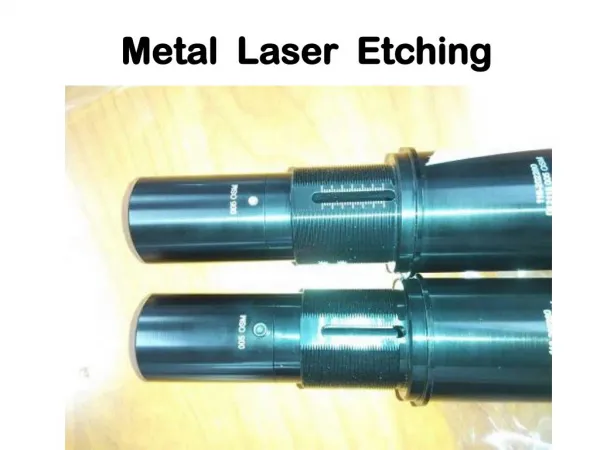
ETCHING
DESCRIPTION
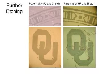
ETCHING. WAFER PROCESS FLOW. DEFINITION. Patterned Etch. Blanket Etch. HISTORY. Adopted in semiconductor industry for transistor & IC manufacture in 1950’s Before 1980, chemical solution were used to dissolve the materials not covered by PR to achieve the pattern transfer
Download
1 / 55
Download Presentation 
ETCHING
An Image/Link below is provided (as is) to download presentation
Download Policy: Content on the Website is provided to you AS IS for your information and personal use and may not be sold / licensed / shared on other websites without getting consent from its author.
Content is provided to you AS IS for your information and personal use only.
Download presentation by click this link.
While downloading, if for some reason you are not able to download a presentation, the publisher may have deleted the file from their server.
During download, if you can't get a presentation, the file might be deleted by the publisher.
E N D
Presentation Transcript
Patterned Etch Blanket Etch
HISTORY • Adopted in semiconductor industry for transistor & IC manufacture in 1950’s • Before 1980, chemical solution were used to dissolve the materials not covered by PR to achieve the pattern transfer • After 1980, replaced by dry (plasma) etch processes


More Related