Download
1 / 88
980 likes | 1.33k Views
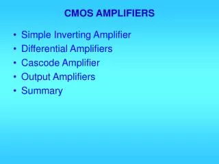
CMOS AMPLIFIERS. Simple Inverting Amplifier Differential Amplifiers Cascode Amplifier Output Amplifiers Summary. Simple Inverting Amplifiers. ACTIVE LOAD INVERTER - VOLTAGE TRANSFER CURVE. Active Load CMOS Inverter Output Swing Limits. But this is not linear operation region!.

E N D
CMOS AMPLIFIERS • Simple Inverting Amplifier • Differential Amplifiers • Cascode Amplifier • Output Amplifiers • Summary
Small Signal Characteristics How do you get better matching?
Large signal characteristic Push-pull
CMOS Push - Pull Inverter Very large signal swing. Not all in linear region
Transfer characteristic Linear region
Small signal High gain!
Transfer function of a system input u output y System
When u(s) = 0, y(s) satisfies: These dynamics are the characteristic dynamics of the system. The roots of the coefficient polynomial are the poles of the system. When y(s) = 0, u(s) satisfies: These dynamics are the zero dynamics of the system. The roots of the coefficient polynomial are the zeros of the system.
Poles of CMOS Inverters Let vin = 0, x = 0, VDD = 0, VSS = 0. CGS1, CGS2, CBS1, CBS2 are all short y CGD1, CGD2, CBD1, CBD2, CL in parallel C’L = Ctotal = CGD1+ CGD2+ CBD1+ CBD2+ CL
Total conductance from y to ground: go = gds1 + gds2 KCL at node y: Therefore system pole is:
Zeros of CMOS Inverters Let vin = x = u, VDD = 0, VSS = 0. CGD1, CGD2, are in parallel, CBD1, CBD2, CL are all short gds1, gds2 also short No current in them KCL: Zero is:
Input output transfer function When s=jw0, A(0) When w∞, A(s)
-3dB frequency of closed loop =b*GB A0=gm/go Acl=1/b 0 dB |p1|= g0/CL’ Unity gain frequency =|A0p1| =GB =gm/CL’ |z1| =gm/Cgd =GB*CL’/Cgd
Unity gain feedback A(s)
If a step input is given, the out put response is In the time domain: Final settling determined by A0 need high gain Settleing speed determined by A0p1=GB, need high gain bandwidth product
Gain bandwidth product C’L = Ctotal = CGD1+ CGD2+ CBD1+ CBD2+ CL When CL ≈ C’L, W↑GB↑, but it saturates, when
Note: If VEB1 and VEB2 are fixed, W1/L1 and W2/L2 must be adjusted proportionally, and they are proportional to DC power.
Therefore: CL constant, but C(W1,W2) proportional to P
GB P
R=total impedance at output node, when vin=0 • C=total capacitance at output node, when Vin=0 • For z, let vout =0, let initial cap volt discharge and compute time constant
Differential Input, single-ended output single stage Amplifier N-Channel vin- vin+
Large Signal Eq. in a N-channel Differential pair =0.5b1(VGS1-VT)2 =(2ID1/b1)0.5 iD1=0, when iD2=ISS and VGS2=VT+(2ISS/b)0.5
Solving for iD1 and iD2 ID1=ID2=ISS/2 VON1=VON2=(ISS/b)0.5
N-Channel Input Pair Differential Amplifier C.M. Load Simple current reference C.M. Bias
INPUT COMMON MODE RANGE VG1=VG2=ViCM VSDSAT1=VSDSAT2 =VON VD1=VD3= VSS+VT3+VON VG1min=VD1-|VT1| VG1max=VDD- VSD5SAT-|VT1|-VON
Common Mode Equivalent Circuit iC1=VIC/(1/gm1 +2rds5) ro1≈1/gm3 ACM≈ 1/ 2rds5gm3 iC1 CMRR=Av/ACM
SLEW RATE: the limit of the rate of change of the output voltage CLdvo/dt=i4-i2 ISS ISS Max |CLdvo/dt| =ISS 0 ISS Slew Rate = ISS/CL
Parasitic Capacitances CT: common mode only CM: mirror cap = Cdg1 + Cdb1 + Cgs3 + Cgs4 + Cdb3 COUT = output cap = Cbd4 + Cbd2 + Cgd2 + CL
Impedances • rout = rsd2 || rds4 = 1 / (gds2 + gds4) • rM = 1/gm3 || rds3 || rds1 ≈ 1/ gm3 • Hence the output node is the high impedance node • When vi=0, slowest discharging node is output node with dominant pole p1 = -1/(C’outrout), where C’out = Cout+ Cgd4 • Approximate transfer function AV(s) = AV/(s/p1─1)
When vG1=vG2=0(AC) KCL at D1: KCL at D2: