Operational Amplifiers
Chapter 8. Operational Amplifiers. Introduction An Ideal Operational Amplifier Basic Operational Amplifier Circuits Other Useful Circuits Real Operational Amplifiers Selecting Component Values Effects of Feedback on Op-amp Circuits. 8.1. Introduction.


Operational Amplifiers
E N D
Presentation Transcript
Chapter 8 Operational Amplifiers • Introduction • An Ideal Operational Amplifier • Basic Operational Amplifier Circuits • Other Useful Circuits • Real Operational Amplifiers • Selecting Component Values • Effects of Feedback on Op-amp Circuits
8.1 Introduction • Operational amplifiers (op-amps) are among the most widely used building blocks in electronics • they are integrated circuits (ICs) • often DIL or SMT
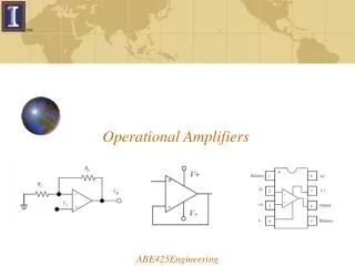
8.2 An Ideal Operational Amplifier • An ideal op-amp would be an ideal voltage amplifier and would have: Av = , Ri= and Ro = 0 Equivalent circuit of an ideal op-amp
8.3 Basic Operational Amplifier Circuits • Inverting and non-inverting amplifiers
When looking at feedback we derived the circuit of an amplifier from ‘first principles’ • Normally we use standard ‘cookbook’ circuits and select component values to suit our needs • In analysing these we normally assume the use of ideal op-amps • in demanding applications we may need to investigate the appropriateness of this assumption • the use of ideal components makes the analysis of these circuits very straightforward
A non-inverting amplifier Analysis Since the gain is assumed infinite, if Vo is finitethen the input voltage must be zero. Hence Since the input resistance of the op-amp is and hence, since V– = V+ = Vi and
Example (see Example 8.1 in the course text) Design a non-inverting amplifier with a gain of 25 From above If G = 25 then Therefore choose R2 = 1 k and R1 = 24 k(choice of values will be discussed later)
An inverting amplifier Analysis Since the gain is assumed infinite, if Vo is finite the input voltage must be zero. Hence Since the input resistance of the op-amp is its input current must be zero, and hence Now
Analysis (continued) Therefore, since I1 = -I2 or, rearranging • Here V– is held at zero volts by the operation of the circuit, hence the circuit is known as a virtual earth circuit
Example (see Example 8.2 in the course text) Design an inverting amplifier with a gain of -25 From above If G = -25 then Therefore choose R2 = 1 k and R1 = 25 k(we will consider the choice of values later)
8.4 Other Useful Circuits • In addition to simple amplifiers op-amps can also be used in a range of other circuits • The next few slides show a few examples of op-amp circuits for a range of purposes • The analysis of these circuits is similar to that of the non-inverting and inverting amplifiers but (in most cases) this is not included here • For more details of these circuits see the relevant section of the course text (as shown on the slide)
8.4.1 • A unity gain buffer amplifier Analysis This is a special case of the non-invertingamplifier with R1 = 0 and R2 = Hence Thus the circuit has a gain of unity • At first sight this might not seem like a very useful circuit, however it has a high input resistance and a low output resistance and is therefore useful as a buffer amplifier
8.4.2 • A current to voltage converter
8.4.3 • A differential amplifier (or subtractor)
8.4.4 • An inverting summing amplifier
8.5 Real Operational Amplifiers • So far we have assumed the use of ideal op-amps • these have Av = , Ri= and Ro = 0 • Real components do not have these ideal characteristics (though in many cases they approximate to them) • In this section we will look at the characteristics of typical devices • perhaps the most widely used general purpose op-amp is the 741
Voltage gain • typical gain of an operational amplifier might be100 – 140 dB (voltage gain of 105 – 106) • 741 has a typical gain of 106 dB (2 105) • high gain devices might have a gain of 160 dB (108) • while not infinite the gain of most op-amps is ‘high-enough’ • however, gain varies between devices and with temperature
Input resistance • typical input resistance of a 741 is 2 M • very variable, for a 741 can be as low as 300 k • the above value is typical for devices based onbipolar transistors • op-amps based on field-effect transistors generally have a much higher input resistance – perhaps 1012 • we will discuss bipolar and field-effect transistors later
Output resistance • typical output resistance of a 741 is 75 • again very variable • often of more importance is the maximum output current • the 741 will supply 20 mA • high-power devices may supply an amp or more
Supply voltage range • a typical arrangement would use supply voltages of +15 V and – 15 V, but a wide range of supply voltages is usually possible • the 741 can use voltages in the range 5 V to 18 V • some devices allow voltages up to 30 V or more • others, designed for low voltages, may use 1.5 V • many op-amps permit single voltage supply operation, typically in the range 4 to 30 V
Output voltage range • the output voltage range is generally determined by the type of op-amp and by the supply voltage being used • most op-amps based on bipolar transistors (like the 741) produce a maximum output swing that is slightly less than the difference between the supply rails • for example, when used with 15 V supplies, the maximum output voltage swing would be about 13 V • op-amps based on field-effect transistors produce a maximum output swing that is very close to the supply voltage range (rail-to-rail operation)
Frequency response • typical 741 frequency response is shown here • upper cut-off frequency is a few hertz • frequency range generally described by theunity-gain bandwidth • high-speed devices may operate up to several gigahertz
8.6 Selecting Component Values • Our analysis assumed the use of an ideal op-amp • When using real components we need to ensure that our assumptions are valid • In general this will be true if we: • limit the gain of our circuit to much less than the open-loop gain of our op-amp • choose external resistors that are small compared with the input resistance of the op-amp • choose external resistors that are large compared with the output resistance of the op-amp • Generally we use resistors in the range 1 k – 100 k
8.7 Effects of Feedback on Op-amp Circuits • Effects of feedback on the Gain • negative feedback reduces gain from A to A/(1 + AB) • in return for this loss of gain we get consistency, provided that the open-loop gain is much greater than the closed-loop gain (that is, A >> 1/B) • using negative feedback, standard cookbook circuits can be used – greatly simplifying design • these can be analysed without a detailed knowledge of the op-amp itself
Effects of feedback on frequency response • as the gain is reduced thebandwidth is increased • gain bandwidth constant • since gain is reduced by (1 + AB) bandwidth is increased by (1 + AB) • for a 741 • gain bandwidth 106 • if gain = 1,000 BW 1,000 Hz • if gain = 100 BW 10,000 Hz
Effects of feedback on input and output resistance • input/output resistance can be increased or decreased depending on how feedback is used. • we looked at this in an earlier lecture • in each case the resistance is changed by a factor of (1 + AB) Example • if an op-amp with a gain of 2 105 is used to produce an amplifier with a gain of 100 then: A = 2 105 B = 1/G = 0.01 (1 + AB) = (1 + 2000) 2000
Example (see Example 8.4 in the course text) • determine the input and output resistance of the following circuit assuming op-amp is a 741 Open-loop gain (A) of a 741 is 2 105 Closed-loop gain (1/B) is 20, B = 1/20 = 0.05 (1 + AB) = (1 + 2 105 0.05) = 104 Feedback senses output voltage therefore it reduces output resistance of op-amp (75 ) by 104 to give 7.5 m Feedback subtracts a voltage from the input, therefore it increases the input voltage of theop-amp (2 M) by 104 to give 20 G
Example (see Example 8.5 in the course text) • determine the input and output resistance of the following circuit assuming op-amp is a 741 Open-loop gain (A) of a 741 is 2 105 Closed-loop gain (1/B) is 20, B = 1/20 = 0.05 (1 + AB) = (1 + 2 105 0.05) = 104 Feedback senses output voltage therefore it reduces output resistance of op-amp (75 ) by 104 to give 7.5 m Feedback subtracts a current from the input, therefore it decreases the input voltage. In this case the input sees R2 to a virtual earth, therefore the input resistance is 1 k
Key Points • Operational amplifiers are among the most widely used building blocks in electronic circuits • An ideal operational amplifier would have infinite voltage gain, infinite input resistance and zero output resistance • Designers often make use of cookbook circuits • Real op-amps have several non-ideal characteristics However, if we choose components appropriately this should not affect the operation of our circuits • Feedback allows us to increase bandwidth by trading gain against bandwidth • Feedback also allows us to alter other circuit characteristics