Download
1 / 24
260 likes | 571 Views
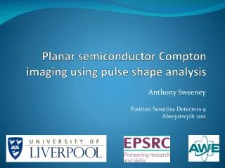
Semiconductor detectors for Compton imaging in nuclear medicine. Laura Harkness ljh@ns.ph.liv.ac.uk PSD9 Conference, Aberystwyth, 12 th September 2011. Outline. Nuclear medicine Compton imaging Design Criteria A High Purity Germanium detector A Si(Li) detector.

E N D
Semiconductor detectors for Compton imaging in nuclear medicine Laura Harkness • ljh@ns.ph.liv.ac.uk PSD9 Conference, Aberystwyth, 12th September 2011
Outline • Nuclear medicine • Compton imaging • Design Criteria • A High Purity Germanium detector • A Si(Li) detector
Nuclear medicine - SPECT Radiopharmaceutical accumulates in organ of interest Gamma-rays emitted from organ and detected outside body by gamma camera Patient injected with radiopharmaceutical Single Photon Emission Computed Tomography (SPECT) Diagnosis/monitoring of cancer and neurological conditions Biological information complements MRI structural information Mechanical collimator 1 x 10 -4 Scintillator detector with photomultiplier tubes
Compton imaging in medicine Source Conventional SPECT Compton imaging Gamma-rays detected by a Compton camera Use 1 gamma ray in every 30 Semiconductor detectors compatible with MRI • Gamma-rays detected by a gamma camera • Inefficient detection method • Use 1 gamma ray in every 3000 • Incompatible with MRI E0 θ E1 θ E2
How does it work? Source • Gamma rays interact in both detectors (scatterer and absorber) • The path for each gamma ray is reconstructed as a cone • Source located at max cone overlap E0 θ E1 θ E2
How does it work? Source • Gamma rays interact in both detectors (scatterer and absorber) • The path for each gamma ray is reconstructed as a cone • Source located at max cone overlap E0 θ E1 θ E2
How does it work? Source • Gamma rays interact in both detectors (scatterer and absorber) • The path for each gamma ray is reconstructed as a cone • Source located at max cone overlap E0 θ E1 θ E2
How does it work? Source • Gamma rays interact in both detectors (scatterer and absorber) • The path for each gamma ray is reconstructed as a cone • Source located at max cone overlap E0 θ E1 θ E2
Design Criteria • L J Harkness et. al, AIP Conf Proc (2009) 1194, 90-95 • System for use with current medical radionuclides, with high sensitivity and excellent image quality • Sensitivity is a factor of: • Detector materials, thicknesses and configuration geometry • Low energy noise thresholds in scatterer detector • Image resolution is a factor of : • Energy resolution • Detector position resolution • Doppler broadening • Detector uniformity Semiconductor Detectors
Final design • L J Harkness et. al, NIMA (2009) 604 • L J Harkness et. al, NIMA (2011) 638 • Optimised for imaging 141 keV gamma rays1 from 99mTc • DSSD Si(Li) scatter detector (two available: 8 mm and 9 mm thick) • DSSD HPGe absorber detector, 20 mm thick • Should operate at the edge of an MRI scanner2 • Final system: 9 mm thick Si(Li) detector and HPGe detector housed in a single cryostat custom-built by STFC Daresbury Laboratory Photo Courtesy of ORTEC Photo Courtesy of Semikon
HPGe Absorber detector MRI images • Each face has 12 strips (60 x 5) mm • 1 test preamplifier for each face of the detector
HPGe Performance Tests MRI images • FWHM measured at 122 keV using a 57Co source • Measurements taken for each channel with: • The source near the AC face of the detector • The source near the DC face of the detector • Specified performance at 122 keV: • Average FWHM <= 1.7 keV • All channels FWHM <= 2.3 keV • No more than 2 strips per side > 1.8 keV
Energy Resolution at 122 keV MRI images • Source near AC face: All channels acceptable (< 2.3 keV) • Source near DC face: All channels acceptable except AC07 Accepted
Energy Resolution at 122 keV MRI images Counts Low Energy Tail? • Specification: Max 2.3 1.7 Energy (keV)
Si(Li) detector • Canberra Si(Li) DSSD detector 13 strips on each face • 8 mm thick, 66 mm diameter • Cryogenically cooled using a CryoPulse CP5 cooler • Energy resolution of all strips measured to be (1.4 to 1.6) keV at 59.4 keV using 241Am (excluding channel 14)
Detector noise levels • L J Harkness et. al, IEEE NSS/MIC Proc (2009) Geant4 Simulation • For imaging 141 keV gamma rays, less than 40 keV is deposited in the scatter detector • Low energy threshold applied reduces the sensitivity • Low noise scatter detector essential in minimising event loss 5keV • Noise levels for DC strips measured to be 2 keV and for AC strips to be (2.5 to 4.5 ) keV
241Am Surface Scan • 1 mm collimated 241Am source scanned in 1 mm steps across a (76 x 76) mm grid giving 5929 positions • Data taken with the source incident on the DC face then the AC face DC face AC face AC Surface scan DC Surface scan
241Am Surface Scan • Data recorded from all 26 channels using Gretina Digitizer cards • DC channels used to trigger the acquisition • Events only recorded when energy deposited in at least one DC channel was more than the energy threshold (~10 keV)
241Am Surface Scan: Event Processing • An 8 keV energy gate was set around the 59.4 keVphotopeak • Events categorised according to fold - the number of channels that record net charge over energy threshold (10 keV for DC channels) • Intensity plots were produced for energy gated events for fold[DC,AC] type events, e.g. fold [1,1].
DC face Intensity Plots Counts reduced by ~8% a) Energy Gated b) Energy Gated Fold [1,1] AC01 Reduced Counts between DC12 & DC13 DC01 DC01 AC13 DC01 DC13
AC face Intensity Plots Counts reduced by ~8% a) Energy Gated b) Energy Gated Fold [1,1] AC01 Reduced Counts between DC12 & DC13 DC01 DC01 AC13 DC01 DC13
Multiple Pixel Intensity Plots a) DC surface scan b) AC surface scan AC01 AC13 DC01 DC13
Current Status and Future Work • HPGe absorber detector: acceptable for Compton imaging. Surface and side scan measurements planned • Further analysis of the Si(Li) detector surface scan results • ProSPECTus cryostat: vacuum testing underway • ProSPECTus Si(Li) detector: acceptance tests imminent • First ProSPECTus imaging measurements –Winter 2011 • ProSPECTus imaging with MRI system – 2012
The ProSPECTus Collaboration Department of Physics, The University of Liverpool, UK AJ Boston, HC Boston, JR Cresswell, DS Judson, PJ Nolan, JA Sampson, DP Scraggs, A Sweeney STFC Daresbury Laboratory, UK I Burrows, N Clague, M Cordwell, J Groves, J Headspith, A Hill, IH Lazarus, V Pucknell, J Simpson MARIARC, The University of Liverpool, UK B Bimson, G Kemp Special Thanks to Hannah Kennedy