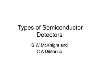
Semiconductor radiation detectors
Semiconductor radiation detectors. Best energy resolutions are obtained by these sensors at present The principle is based on the generation of electron-hole pairs by the incident radiation, which are then collected by applying a voltage across two contacts


Semiconductor radiation detectors
E N D
Presentation Transcript
Semiconductor radiation detectors • Best energy resolutions are obtained by these sensors at present • The principle is based on the generation of electron-hole pairs by the incident radiation, which are then collected by applying a voltage across two contacts • Since the ionization voltage is only a few eV compared to 10s of eV for typical gases, so the efficiency of ion generation is much higher. This means higher energy resolution. • There are several desirable properties for semiconductors that are needed for detection: • Excellent charge transport (high mobility) • Low leakage current of darkj current • Efficient production of electron-hole pairs due to radiation • Fast response • Low cost • Radiation tolerance • Ge and Si are good choices for radiation detection, • but the former needs to be cooled, while the later is • not good for detection (why?). • A special geometry is needed to maximize radiation • collection area so a cylindrical geometry is generally • preferred. Lithium-drifted pin-junction detector. Structure of the detector (a) and coaxial configuration of the detector (b)
Semiconductor radiation detectors: New trends • One of the latest semiconductor materials for radiation detection are CdTe and CdZnTe • They offer high enough band gap of 1.5 eV (low dark current at room temp, resistivity up to 1010 cm-3), and also large average Z of the constituent atoms for efficient interaction with -ray, and production of electron-hole pairs • The principal challenges are poor material quality, which leads to performance challenges. Not yet comparable to cooled Ge detectors. Detector with 20x20x10mm CZT crystal showing planar cathode and guard ring. (Courtesy of Quik-Pak, a division of Delphon Industries)
Chemical and biological sensors: Classification • Based on electrical and electrochemical properties • Metal oxide semiconductor based • Electrochemical sensors • Potentiometric sensors • Conductometric sensors • Amperometric sensors • Chem-FET • Based on Changes in physical properties • Mass change • Stress change • Work function change • Capacitance change • Thermal conductivity change • Based on Optical property changes • Luminescence • Transmittance/Absorption • Complex array based sensors for multiplexed detection
Chemical and biological analytes: Classification • Toxic gases and pollutants (NOx, SO2, NH3, O3, heavy metal, As) • Volatile organic compounds (alcohol, toluene, benzene) • Explosives (TNT, PETN, RDX) • Chemical warfare agents (Sarin, Tabun, Mastard gas) • Bio-analytes • Blood parameters (urea, pH, lactic acid, glucose, pO2) • Pathogens (virus, bacteria, fungi, proteins) • Cancer/Tumor cells • Specific disease markers (PSA) • Intracellular matter (DNA, RNA, proteins)
Single and array based detection Metal-oxide-semiconductor-based sensor response to increasing and decreasing concentrations of ethanol Response of a capacitive VOC sensor array containing seven differently absorbing polymer-coated chemicapacitors to pulses of acetone, methyl ethyl ketone, toluene, ethanol, and water at 25 C
Sensor parameters • Sensitivity (usually ppb, sometimes even ppt) • Selectivity • Response time (seconds to minutes) • Repeatability • Lifetime (at least 1 year) All these parameters are expected to get better with nanoscale material. Why?