Microprogramming Project
Microprogramming Project. You are to write and submit a microprogram to interpret the following target machine instruction set on a given datapath using the microprogramming tool “A Microprogramming Simulation System” (AMISS).


Microprogramming Project
E N D
Presentation Transcript
Microprogramming Project • You are to write and submit a microprogram to interpret the following target machine instruction set on a given datapath using the microprogramming tool “A Microprogramming Simulation System” (AMISS). • AMISS is run at the command line on Grace while in the directory where your microprogram memory control file "cmemory”, and test program “memory” reside as follows: ~meseec/AMISS/CPU -d • You are required to to e-mail your fully-commented "cmemory", "memory" files containing the machine instruction programs that you have used to test your control microprogram to: “meseec@rit.edu” • In addition to submitting your "cmemory" and " memory files by e-mail, you should submit a written report with the following items: (1) A brief description of your approach to the assignment, and the features of your solution. (2) Dependent RTN statements for all the instructions implemented. (3) The resulting CPI for the different instruction types. (4) A statement of any relevant problems or difficulties encountered during the assignment. (5) A listing of your fully-commented "cmemory" and " memory" files as e-mailed. (6) A description of testing procedures used and observations. (7) Any additional remarks or conclusions you deem noteworthy of mention. Due February 23
Opcode Opcode Opcode Data Byte AddressLo AddressHi Target Instruction Set Architecture (ISA) • The target ISA is an 8-bit Accumulator-based ISA with variable length encoding (1-3 bytes). • 16-bit memory addressing: • Total addressable memory = 216 = 64 KBytes = 65536 Bytes (for program, data, stack space) • There are three types of instructions supported: (1) Inherent instructions: One-byte instructions, just the Opcode byte. (2) Immediate instructions: Two-byte instructions. The instruction Opcode byte is followed by one additional byte of immediate data. (3) Memory reference instructions: three-byte instructions. The instruction Opcode byte is followed by two bytes of address information. The high-order byte of the address appears in the byte memory location immediately following the Opcode byte (Big Endian order).
PC SP PCHi PCLo SPHi SPLo Acc ISA Registers & Flags • 16-bit Program Counter (PC) • 8-bit Accumulator • 16-bit Stack Pointer (SP) • Four Flags or condition code bits NZVC N = Negative Flag Z = Zero Flag V = Overflow Flag C = Carry Flag • The effect of an instruction on the flags is indicated by "0" for flag is cleared (i.e. = 0) "1" for flag is set (i.e = 1) "-" for no change, and "x" for possible flag value change according to instruction result
Opcode Instruction Types:Inherent Instructions: One Byte Only Opcode Effect on Flags: NZVC 00001111 - NOP - No operation - - - - 00011111 - HALT - Halt the machine - - - - 00101111 - CLA - Clear the accumulator 0100 00111111 - CMA - 1’s complement the accumulator xx00 01001111 - INCA - Increment the accumulator by one xx0x 01011111 - DECA - Decrement the accumulator by one xx0x 01101111 - RET - Return from subroutine - - - - (post incrementing SP) 01111111 - ROLCA - Circular shift Carry bit & Acc left 1 bit xx0x 10001111 - CLC - Clear Carry Flag bit - - - 0 10011111 - STC - Set Carry Flag bit - - - 1 Instruction
Inherent Instructions Opcodes Binary Hex NOP 00001111 0f HALT 00011111 1f CLA 00101111 2f CMA 00111111 3f INCA 01001111 4f DECA 01011111 5f RET 01101111 6f ROLCA 01111111 7f CLC 10001111 8f STC 10011111 9f Instruction Types:Inherent Instructions Opcodes
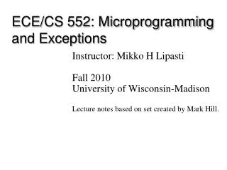
AC6 AC0 AC0 AC2 AC3 AC4 AC5 AC1 AC1 AC6 AC5 AC4 AC3 AC7 AC2 C Opcode Inherent Instructions Example:ROLCA - Circular shift Carry bit & Acc left 1 bit Independent RTN: Instruction ¬ Mem[PC] PC ¬ PC + 1 C ¬ AC7 ; Accumulator ¬ AC6 AC5 AC4 AC3 AC1 AC1 ACo C 01111111 = 7f (Hex) Before ROLCA: Accumulator Carry Flag C C After ROLCA: Accumulator Carry Flag C AC7
Opcode Instruction AddressLo AddressHi Instruction Types:Store and Branch Instructions: Two additional address bytes Opcode Effect on Flags: NZVC 00001z00 - STA - Store accumulator (use STAin for indirect) - - - - 00011z00 - JMP - Unconditional branch - - - - 00101z00 - JEQ - Branch if equal to zero (Z=1) - - - - 00111z00 - JCS - Branch if carry (C=1) - - - - 01001z00 - JLT - branch if negative (N=1) - - - - 01011z00 - JVS - branch if overflow (V=1) - - - - 01101z00 - JSR - jump to subroutine - - - - (push PC on stack - predecrement SP) The z bit in the instruction Opcode determines the addressing mode used: z = 0 Direct addressing, the address needed follows the Opcode z = 1 Indirect addressing, the address following the Opcode is a pointer to the address needed by the instruction
Store and Branch Instructions Opcodes Binary Hex (Direct z=0) (Indirect z=1) STA 00001z00 08 0c JMP 00011z00 18 1c JEQ 00101z00 28 2c JCS 00111z00 38 3c JLT 01001z00 48 4c JVS 01011z00 58 5c JSR 01101z00 68 6c Instruction Types:Store and Branch Instructions Opcodes
AddressHi AddressLo Opcode Opcede = 0b Address 00001000 = 08 (Hex) Accumulator Example Instruction STA Store AccumulatorDirect (z=0 in Opcode) AddressLo AddressHi Store and Branch Instructions Addressing Modes:Direct Addressing . . . . Store Accumulator at address Independent RTN: Instruction ¬ Mem[PC] AddressHi ¬ Mem[PC + 1] AddressLo ¬ Mem[PC + 2] PC ¬ PC + 3 Mem[Address] ¬ Accumulator Low Memory
Example Instruction STAind Store AccumulatorIndirect (z=1 in Opcode) Address 00001100 = 0c (Hex) AddressLo Opcode Opcede = 0f AddressLo AddressHi AddressHi Accumulator AddressLo AddressHi Store and Branch Instructions Addressing Modes:Indirect Addressing . . . . Store Accumulator at indirect address Independent RTN: Instruction ¬ Mem[PC] AddressHi ¬ Mem[PC + 1] AddressLo ¬ Mem[PC + 2] PC ¬ PC + 3 Mem[ Mem[Address] ] ¬ Accumulator Low Memory
Stack Opcode PCHi PCLo Subroutine Address 01101000 = 68 (Hex) Instruction JSR Direct (z=0 in Opcode) AddressLo Low Memory AddressHi Subroutine Call/Return & Stack Operation • The Stack Pointer (SP) points to the last filled byte in the stack and is initialized in high memory • The stack grows to low memory as items are added • JSR - Jump to Subroutine Direct (push PC on stack - predecrement SP) Initial SP Independent RTN: Instruction ¬ Mem[PC] AddressHi ¬ Mem[PC + 1] Get Subroutine Address AddressLo ¬ Mem[PC + 2] PC ¬ PC + 3 SP ¬ SP - 2 Predecrement Stack Pointer by 2 Mem[SP] ¬ PCHi Push return address on the stack Mem[SP+1] ¬ PCLo PC ¬ AddressHi, AddressLo Go to subroutine SP after JSR (decremented by 2)
Instruction RET Opcode 01101111 = 6f (Hex) Stack PCHi PCLo Initial SP SP after RET (Incremented by 2) Low Memory Subroutine Call/Return & Stack Operation RET- Return from Subroutine (post incrementing SP) Independent RTN: Instruction ¬ Mem[PC] PC ¬ PC + 1 PCHi ¬ Mem[SP] Get Subroutine Address PCLo ¬ Mem[SP + 1] SP ¬ SP + 2 Post increment Stack Pointer(SP) by 2
Instruction Types:“Other” Instructions: One or Two Additional Bytes Opcode Effect on Flags: NZVC 0000yz01 - LDA - Load Acc (use LDAim for immediate) xx00 0001yz01 - ORA - Inclusive OR to Accumulator xx00 0010yz01 - EOR - Exclusive OR to Accumulator xx00 0011yz01 - AND - Logical AND to Accumulator xx00 0100yz01 - ADD - Add to Accumulator xxxx 0101yz01 - SUBA - Subtract from Accumulator xxxx 0110yz01 - LDS - Load stack pointer SP with 16-bit value - - - - The yz bits in the instruction Opcode determine the addressing mode used: y = 0, z = 0 Direct addressing, the address of operand needed follows the Opcode y = 1, z = 0 Immediate addressing, the one or two byte operands follows the Opcode y = 0, z = 1 Indirect addressing, the address following the Opcode is a pointer to the address needed by the instruction y =1, z = 1 Not allowed, illegal Opcode
Other Instructions Opcodes Binary Hex Direct Indirect Immediate y = z =0 y=0 z =1 y=1 z=0 LDA 0000yz01 01 05 09 ORA 0001yz01 11 15 19 EOR 0010yz01 21 25 29 AND 0011yz01 31 35 39 ADD 0100yz01 41 45 49 SUBA 0101yz01 51 55 59 LDS 0110yz01 61 65 69 Instruction Types:“Other” Instructions Opcodes
Operand Opcede = 08 Opcode Accumulator Data Byte “Other” Instructions Addressing Modes:Immediate Addressing LDA 0000yz01 Example Instruction LDAImm AccumulatorImmediate (y = 1 z = 0 in Opcode) Operand 00001001 = 09 (Hex) . . . . Load Accumulator With immediate operand after opcode Independent RTN: Instruction ¬ Mem[PC] Accumulator ¬ Mem[PC + 1] PC ¬ PC + 2 Low Memory
AddressHi AddressLo Opcede = 00 Opcode Accumulator AddressLo AddressHi “Other” Instructions Addressing Modes:Direct Addressing LDA 0000yz01 Example Instruction LDA Accumulator (y = 0 z = 0 in Opcode) Address 00000001 = 00 (Hex) . . . . Load Accumulator with byte at address Independent RTN: Instruction ¬ Mem[PC] AddressHi ¬ Mem[PC + 1] AddressLo ¬ Mem[PC + 2] PC ¬ PC + 3 Accumulator ¬ Mem[Address] Low Memory
Example Instruction LDAind Load AccumulatorIndirect (y = 0 z = 1 in Opcode) Address 00000100 = 05 (Hex) AddressHi AddressLo AddressLo Opcode AddressHi Opcede = 04 Accumulator AddressLo AddressHi “Other” Instructions Addressing Modes: Indirect Addressing LDA 0000yz01 . . . . Load Accumulator with byte at indirect address Independent RTN: Instruction ¬ Mem[PC] AddressHi ¬ Mem[PC + 1] AddressLo ¬ Mem[PC + 2] PC ¬ PC + 3 Accumulator ¬ Mem[ Mem[Address] ] Low Memory
The Datapath X Y
Datapath Details • ISA Registers: • Program Counter (PC) 16 bits implemented in datapath by two 8-bit registers: PCHi, PCLo • Accumulator (ACC) 8-bit register. • Flags Register (FLGS) 8-bit register, low four bits are the flags: NZVC • Stack Pointer (SP) 16-bit register implemented in datapath by two 8-bit registers: SPHi, SPLo • Memory Details • A single main memory used for instructions and data. 16-bit address. • Memory Address High Register (MAH) must be loaded first for both reads and writes. • For memory writes the MW (Memory Write) register must be loaded with the byte to be stored. • Reading from and writing to memory is triggered by loading MAL (Memory Address Low) register using ALUDEST microinstruction field options. • Memory read/write operations take two clock cycles from the start of a memory read or write. • Temporary Datapath/Microprogram Registers: • The following 8 -bit registers can be used by the control microprogram to store temporary values as needed and are not visible to the ISA or user programs: T, U, B, XLo, Xhi • The ALU Output Shifter: • Combinational logic shifter that can shift the ALU output one position left or right and also manipulate the most significant bit of the ALU output (L-bit) before shifting in a single cycle. • Constant Value (Const): • Shown as a possible input to the ALU is 5-bit value that can be specified by a microinstruction field (field H).
A B C D E F G H I J K L M N MEMDEST LCNTRL SHFTCTRL ALUCTRL YSOURCE XSOURCE ALUDEST CONST LOADFLGS TEST INTERNAB ADDRF COND OPCODE Bits 30-38 Bits 39-40 Bits 41-42 (9 bits) (2 bits) (2 bits) Bits 0-1 Bits 2-3 Bits 4-5 Bits 6-9 Bits 10-13 Bits 14-16 Bits 17-20 Bits 21-25 Bit 26 Bits 27-28 Bit 29 (2 bits) (2 bits) (2 bits) (4 bits) (4 bits) (3 bits) (4 bits) (5 bits) (1 bit) (2 bits) (1 bit) The Microinstruction Format Bit Field Name Operations 00 (0) - NOP (See Note 2) 01 (1) - MD 10 (2) - MD and MALow 11 (3) - MD and MALow and IR 0 1 2 3 4 5 6 7 8 9 10 11 12 13 14 15 16 A MEMDEST 00 (0) - Leave L alone 01 (1) - Clear L 10 (2) - Set L 11 (3) - L = Carry Out of ALU B LCNTRL C SHFTNTRL 00 (0) - No Shift 01 (1) - Shift Right 10 (2) - Shift Left 11 (3) - Not Used 0000 (0) - X 0001 (1) - Y 0010 (2) - X plus Y 0011 (3) - X plus Y plus 1 0100 (4) - X and Y 0101 (5) - X or Y 0110 (6) - X xor Y 0111 (7) - not Y 1000 (8) - X plus 1 1001 (9) - Y plus 1 1010 (10) - X and 1 1011 (11) - Y and 1 1100 (12) - Y plus not X plus 1 1101 (13) - not X 1110 (14) - minus 1 1111 (15) - 0 D ALUCTRL E YSOURCE 0000 (0) - none 0001 (1) - ACC 0010 (2) - PCLo 0011 (3) - SPLo 0100 (4) - B 0101 (5) - FLAGS 0110 (6) - XHi 0111 (7) - XLo 1000 (8) - PCHi 1001 (9) - SPHi 1010 (10) - unused 1011 (11) - unused 1100 (12) - unused 1101 (13) - unused 1110 (14) - unused 1111 (15) - unused 000 (0) - ACC 001 (1) - MD 010 (2) - CONST (Constant Field from Microinstruction) 011 (3) - External Data (not used here) 100 (4) - T 101 (5) - MALo 110 (6) - MAHi 111 (7) - U F XSOURCE Field values above = Binary (Decimal) - Functionality All microinstruction field values in cmemory file must in decimal
A B C D E F G H I J K L M N MEMDEST LCNTRL SHFTCTRL ALUCTRL YSOURCE XSOURCE ALUDEST CONST LOADFLGS TEST INTERNAB ADDRF COND OPCODE Bits 30-38 Bits 39-40 Bits 41-42 (9 bits) (2 bits) (2 bits) Bits 0-1 Bits 2-3 Bits 4-5 Bits 6-9 Bits 10-13 Bits 14-16 Bits 17-20 Bits 21-25 Bit 26 Bits 27-28 Bit 29 (2 bits) (2 bits) (2 bits) (4 bits) (4 bits) (3 bits) (4 bits) (5 bits) (1 bit) (2 bits) (1 bit) The Microinstruction Format Bit Field Name Operations G ALUDEST 0000 (0) - none 0001 (1) - ACC 0010 (2) - PCLo 0011 (3) - SPLo 0100 (4) - B 0101 (5) - FLAGS 0110 (6) - XHi 0111 (7) - XLo 1000 (8) - PCHi 1001 (9) - SPHi 1010 (10) - MAHi 1011 (11) - MALo, Read (Starts Memory Read) 1100 (12) - T 1101 (13) - MALo, Write (Starts Memory Write) 1110 (14) - U 1111 (15) - MW 17 18 19 20 21 22 23 24 25 26 H CONST Unsigned 5-bit constant for XSOURCE Value Range: 00000-11111 (0-31) I LOADFLGS When 1 loads FLAGS from internal ALU flags NBIT, ZBIT, VBIT, CBIT 00 (0) - Branch on NBIT (See Note 1) 01 (1) - Branch on ZBIT 10 (2) - Branch on VBIT 11 (3) - Branch on CBIT 27 28 29 30 31 32 33 34 35 36 36 38 39 40 41 42 J TEST Not Used, always put 0 in this field K INTRENAB L ADDRF 9-bit address field of Next microinstruction bit 30: Most Significant Bit of Address (See Note 1) Address range: 0-511 (Decimal) M COND Determines Type of Next Microinstruction Address (See note 1) Opcode: Format of Microinstruction Only one format used here, always put 0 in this field. N OPCODE Field values above = Binary (Decimal) - Functionality All microinstruction field values in cmemory file must in decimal
A B C D E F G H I J K L M N MEMDEST LCNTRL SHFTCTRL ALUCTRL YSOURCE XSOURCE ALUDEST CONST LOADFLGS TEST INTERNAB ADDRF COND OPCODE Bits 30-38 Bits 39-40 Bits 41-42 (9 bits) (2 bits) (2 bits) Bits 0-1 Bits 2-3 Bits 4-5 Bits 6-9 Bits 10-13 Bits 14-16 Bits 17-20 Bits 21-25 Bit 26 Bits 27-28 Bit 29 (2 bits) (2 bits) (2 bits) (4 bits) (4 bits) (3 bits) (4 bits) (5 bits) (1 bit) (2 bits) (1 bit) Micrinstruction Fields Notes • Note 1: • If COND = 00 (0 decimal) then MPC (next microinstruction address) = ADDRF (i.e bits 30-38) as given • If COND = 01 (1 decimal) Then MPC (next microinstruction address) is determined by bits 30-37 of ADDRF along • with the particular test bit specified by TEST field from the ALU replacing the least significant bit • of 38 of ADDRF (i.e two way branch on the condition bit tested). • If COND = 10 (2 decimal) Then MPC (next microinstruction address) by bits 30-34 (five most significant bits of • ADDRF) along with the 4 most significant bits of IR (instruction register) replacing the low 4 bits • 35-38 of ADDRF (I.e 16-way branch on the 4 most significant bits of IR). • If COND = 11 (3 decimal) Then MPC (next microinstruction address) by bits 30-34 (five most significant bits of • ADDRF) along with the 4 least significant bits of IR (instruction register) replacing the low 4 bits • 35-38 of ADDRF (I.e 16-way branch on the 4 least significant bits of IR). • Note 2: The Memory destination from the memory bus MBUS (memory data bus) is as follows: • When the MEMDEST field is not 00 (0 decimal), MD is loaded from MBUS. • When the field is 10 (2 decimal), MD and MALo registers are loaded from MBUS • When the field is 11 (3 decimal) MD, MALo and IR registers are loaded from MBUS • Note 3: For every microinstruction field, use the decimal value of the binary field values specified above, as • shown in the sample microprogram start segment on the next page. • Note 4: A microinstruction with each field filled with 999 will halt execution.
Six Types of Instructions According to Low-Half of Opcode • Inherent Instructions: Low half of Opcode = 1111 = f (hex) • One Byte: Opcode • Store/Branch (S/B) Direct: Low half of Opcode = 1000 = 8 (hex) • Opcode, two direct address bytes following opcode • Store/Branch (S/B) Indirect: Low half of Opcode = 1100 = c (hex) • Opcode, two indirect address bytes following opcode • Need to get two more bytes of address • “Other” Direct: Low half of Opcode = 0001 = 1 (hex) • Opcode, two bytes of direct address of operand following opcode • Direct address is then used to fetch operand byte (or two bytes in case of LDS) • “Other” Indirect: Low half of Opcode = 0101 = 5 (hex) • Opcode, two indirect bytes of address following opcode • Need to get two more bytes of address of operand • Operand address is then used to fetch operand byte (or two bytes in case of LDS) • “Other” Immediate: Low half of Opcode = 1001 = 9 (hex) • Opcode, followed with one byte of operand (or two bytes in case of LDS) 0 1 2 3 4 5 6 7 8 9 A B C D E F Inherent (S/B) Indirect (S/B) Direct “Other” Direct “Other” Indirect “Other” Immediate Low Half of Opcode Byte
Inherent (S/B) Indirect (S/B) Direct “Other” Direct “Other” Indirect “Other” Immediate Get address bytes following opcode 16 way-branch on upper half of opcode Get indirect address bytes following opcode and then use to get address needed Get address bytes following opcode and use to get operand Get indirect address bytes following opcode and use to get address of operand and get operand Get operand bytes following opcode 16 way-branch on upper half of opcode Complete Instruction 16 way-branch on upper half of opcode 16 way-branch on upper half of opcode 16 way-branch on upper half of opcode Complete Instruction 16 way-branch on upper half of opcode Complete Instruction Complete Instruction Complete Instruction Complete Instruction A Possible High-Level Microprogram Flow Initialize PC, SP, ACC Fetch Opcode, Update PC Start Decode 16 way-branch on low half of opcode 1 5 8 9 C F
Sample Microprogram Start Segment Includes: initialization Opcode fetch, partial decode ;A - MEMDEST ;| B - LCNTRL ;| | C - SHFTCNTRL ;| | | D - ALUCNTRL ;| | | | E - YSRCE ;| | | | | F - XSRCE ;| | | | | | G - ALUDEST ;| | | | | | | H - CONST ;| | | | | | | | I - LDFLG ;| | | | | | | | | J - TEST ;| | | | | | | | | | K - INTRNE ;| | | | | | | | | | | L - ADDR ;| | | | | | | | | | | | M - COND ;| | | | | | | | | | | | | N - OPCODE ;| | | | | | | | | | | | | | ADDRESS COMMENT 0 0 0 15 0 0 8 0 0 0 0 1 0 0; 000 :PCHI <- 0 0 0 0 15 0 0 2 0 0 0 0 2 0 0; 001 :PCLO <- 0 0 0 0 13 0 2 9 0 0 0 0 3 0 0; 002 :SPHI <- FF 0 0 0 13 0 2 3 0 0 0 0 4 0 0; 003 :SPLO <- FF 0 0 0 15 0 0 1 0 4 0 0 5 0 0; 004 :ACC <- 0 0 0 0 1 8 0 10 0 0 0 0 6 0 0; 005 :MAHI <- PCHI 0 0 0 1 2 0 11 0 0 0 0 7 0 0; 006 :MALO <- PCLO START FETCH 0 0 0 9 2 0 2 0 0 3 0 8 1 0; 007 :PCLO += 1 (ALSO WAIT CYCLE) 3 0 0 0 0 0 0 0 0 0 0 10 0 0; 008 :IR <- M 3 0 0 9 8 0 8 0 0 0 0 10 0 0; 009 :IR <- M, PCHI+=1 ;END OPCODE FETCH, START DECODE
Sample Microprogram Start Segment(Continued) ;A - MEMDEST ;| B - LCNTRL ;| | C - SHFTCNTRL ;| | | D - ALUCNTRL ;| | | | E - YSRCE ;| | | | | F - XSRCE ;| | | | | | G - ALUDEST ;| | | | | | | H - CONST ;| | | | | | | | I - LDFLG ;| | | | | | | | | J - TEST ;| | | | | | | | | | K - INTRNE ;| | | | | | | | | | | L - ADDR ;| | | | | | | | | | | | M - COND ;| | | | | | | | | | | | | N - OPCODE ;| | | | | | | | | | | | | | ADDRESS COMMENT ;END OPCODE FETCH, START DECODE 0 0 0 0 0 0 0 0 0 0 0 16 3 0; 010 :START DECODE 0 0 0 0 0 0 0 0 0 0 0 16 0 0; 011 :NO-OP 0 0 0 0 0 0 0 0 0 0 0 16 0 0; 012 :NO-OP 0 0 0 0 0 0 0 0 0 0 0 16 0 0; 013 :NO-OP 0 0 0 0 0 0 0 0 0 0 0 16 0 0; 014 :NO-OP 0 0 0 0 0 0 0 0 0 0 0 16 0 0; 015 :NO-OP ;BEGIN FIRST STAGE DECODE, 16-WAY BRANCH ON LOWER HALF OF OPCODE BYTE 0 0 0 0 0 0 0 0 0 0 0 349 0 0; 016 :NO-OP ERROR HALt 0 0 0 0 0 0 0 0 0 0 0 144 0 0; 017 :NO-OP DIRECT OTHER 0 0 0 0 0 0 0 0 0 0 0 349 0 0; 018 :NO-OP ERROR HALT 0 0 0 0 0 0 0 0 0 0 0 349 0 0; 019 :NO-OP ERROR HALT 0 0 0 0 0 0 0 0 0 0 0 349 0 0; 020 :NO-OP ERROR HALT 0 0 0 0 0 0 0 0 0 0 0 192 0 0; 021 :NO-OP INDIRECT OTHER 0 0 0 0 0 0 0 0 0 0 0 349 0 0; 022 :NO-OP ERROR HALT 0 0 0 0 0 0 0 0 0 0 0 349 0 0; 023 :NO-OP ERROR HALT 0 0 0 0 0 0 0 0 0 0 0 96 0 0; 024 :NO-OP DIRECT S/B 0 0 0 0 0 0 0 0 0 0 0 208 0 0; 025 :NO-OP IMMEDIATE OTHER 0 0 0 0 0 0 0 0 0 0 0 349 0 0; 026 :NO-OP ERROR HALT 0 0 0 0 0 0 0 0 0 0 0 349 0 0; 027 :NO-OP ERROR HALT 0 0 0 0 0 0 0 0 0 0 0 64 0 0; 028 :NO-OP INDIRECT S/B 0 0 0 0 0 0 0 0 0 0 0 349 0 0; 029 :NO-OP ERROR HALT 0 0 0 0 0 0 0 0 0 0 0 349 0 0; 030 :NO-OP ERROR HALT 0 0 0 0 0 0 0 0 0 0 0 32 2 0; 031 :NO-OP INHERNET;END FIRST STAGE DECODE, BEGIN SECOND STAGE ; 999 999 999 999 999 999 999 999 999 999 999 999 999 999; 349: HALT