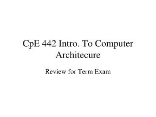
CpE 442 Microprogramming and Exceptions
CpE 442 Microprogramming and Exceptions. Review of a Multiple Cycle Implementation. The root of the single cycle processor’s problems: The cycle time has to be long enough for the slowest instruction Solution: Break the instruction into smaller steps


CpE 442 Microprogramming and Exceptions
E N D
Presentation Transcript
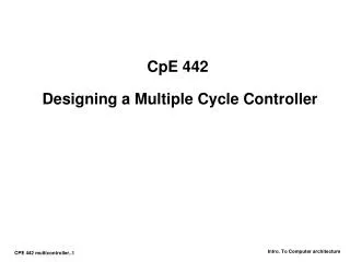
Review of a Multiple Cycle Implementation • The root of the single cycle processor’s problems: • The cycle time has to be long enough for the slowest instruction • Solution: • Break the instruction into smaller steps • Execute each step (instead of the entire instruction) in one cycle • Cycle time: time it takes to execute the longest step • Keep all the steps to have similar length • This is the essence of the multiple cycle processor • The advantages of the multiple cycle processor: • Cycle time is much shorter • Different instructions take different number of cycles to complete • Load takes five cycles • Jump only takes three cycles • Allows a functional unit to be used more than once per instruction
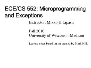
Target 32 0 Mux 0 Mux 1 ALU 0 1 Mux 32 1 ALU Control Mux 1 0 << 2 Extend 16 Review: Multiple Cycle Datapath PCWr PCWrCond PCSrc BrWr Zero ALUSelA IorD MemWr IRWr RegDst RegWr 1 Mux 32 PC 0 Zero 32 Rs Ra 32 RAdr 5 32 Rt Rb busA 32 Ideal Memory 32 Instruction Reg Reg File 5 32 4 Rt 0 Rw 32 WrAdr 32 1 32 Rd Din Dout busW busB 32 2 32 3 Imm 32 ALUOp ExtOp MemtoReg ALUSelB
Overview of the Two Lectures • Control may be designed using one of several initial representations. The choice of sequence control, and how logic is represented, can then be determined independently; the control can then be implemented with one of several methods using a structured logic technique. Initial Representation Finite State Diagram Microprogram Sequencing Control Explicit Next State Microprogram counter Function + Dispatch ROMs Logic Representation Logic Equations Truth Tables Implementation Technique PLA ROM “hardwired control” “microprogrammed control”
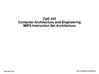
Ifetch Rfetch/Decode BrComplete ALUOp=Add 1: PCWr, IRWr ALUOp=Add ALUOp=Sub x: PCWrCond 1: BrWr, ExtOp ALUSelB=01 RegDst, Mem2R ALUSelB=10 x: IorD, Mem2Reg Others: 0s RegDst, ExtOp x: RegDst, PCSrc IorD, MemtoReg 1: PCWrCond ALUSelA Others: 0s PCSrc RExec 1: RegDst ALUSelA ALUOp=Or ALUSelB=01 1: ALUSelA ALUOp=Rtype ALUSelB=11 x: PCSrc, IorD MemtoReg x: MemtoReg ExtOp IorD, PCSrc Rfinish 1: ALUSelA ALUOp=Rtype ALUOp=Or RegWr, ExtOp 1: RegDst, RegWr MemtoReg x: IorD, PCSrc ALUselA ALUSelB=11 ALUSelB=11 ALUSelB=01 ALUOp=Add 1: ALUSelA x: IorD, PCSrc x: PCSrc RegWr ExtOp IorD Initial Representation: Finite State Diagram 0 1 8 beq 2 AdrCal 1: ExtOp ALUSelA ALUSelB=11 lw or sw ALUOp=Add x: MemtoReg Ori PCSrc 10 Rtype lw sw OriExec 3 6 5 SWMem LWmem 1: ExtOp ALUSelA, IorD 1: ExtOp MemWr ALUSelB=11 ALUSelA ALUOp=Add ALUSelB=11 x: MemtoReg ALUOp=Add PCSrc x: PCSrc,RegDst 11 MemtoReg OriFinish 7 4 LWwr
Opcode Sequencing Control: Explicit Next State Function O u t p u t s Control Logic • Next state number is encoded just like datapath controls Multicycle Datapath Inputs State Reg
S3 S2 S1 S0 NS3 NS2 NS1 NS0 Implementation Technique: Programmed Logic Arrays • Each output line the logical OR of logical AND of input lines or their complement: AND minterms specified in top AND plane, OR sums specified in bottom OR plane lw = 100011 sw = 101011 R = 000000 ori = 001011 beq = 000100 jmp = 000010 Op5 Op4 Op3 Op2 Op1 Op0 0 = 0000 1 = 0001 2 = 0010 3 = 0011 4 = 0100 5 = 0101 6 = 0110 7 = 0111 8 = 1000 9 = 1001 10 = 1010 11 = 1011
State Reg Opcode Sequencer-based control unit details Control Logic Inputs Dispatch ROM 1 Op Name State 000000 Rtype 0110000010 jmp 1001000100 beq 1000001011 ori 1010 100011 lw 0010101011 sw 0010 Dispatch ROM 2 Op Name State 100011 lw 0011101011 sw 0101 1 Adder Mux 3 2 1 0 0 Address Select Logic ROM2 ROM1
Implementing Control with a ROM • Instead of a PLA, use a ROM with one word per state (“Control word”) State number Control Word Bits 18-2 Control Word Bits 1-0 0 10010100000001000 11 1 00000000010011000 01 2 00000000000010100 10 3 00110000000010100 11 4 00110010000010110 00 5 00101000000010100 00 6 00000000001000100 11 7 00000000001000111 00 8 01000000100100100 00 9 10000001000000000 00 10 … 11 11 … 00
Macroinstruction Interpretation User program plus Data this can change! Main Memory ADD SUB AND . . . one of these is mapped into one of these DATA execution unit AND microsequence e.g., Fetch Calc Operand Addr Fetch Operand(s) Calculate Save Answer(s) CPU control memory
Variations on Microprogramming ° Horizontal Microcode – control field for each control point in the machine ° Vertical Microcode – compact microinstruction format for each class of microoperation branch: µseq-op µadd execute: ALU-op A,B,R memory: mem-op S, D µseq µaddr A-mux B-mux bus enables register enables
Microprogramming Pros and Cons • Ease of design • Flexibility • Easy to adapt to changes in organization, timing, technology • Can make changes late in design cycle, or even in the field • Can implement very powerful instruction sets (just more control memory) • Generality • Can implement multiple instruction sets on same machine. (Emulation) • Can tailor instruction set to application. • Compatibility • Many organizations, same instruction set • Costly to implement • Slow
Outline of Today’s Lecture • Recap (5 minutes) • Microinstruction Format Example (15 minutes) • Do-it-yourself Microprogramming (25 minutes) • Exceptions (25 minutes)
Designing a Microinstruction Set • Start with the list of control signals • Group signals together in groups that make sense: called “fields” • Places fields in some logical order (ALU operation & ALU operands first and microinstruction sequencing last) • Create a symbolic legend for the microinstruction format, showing name of field values and how they set the control signals • To minimize the width, encode operations that will never be used at the same time
Start with list of control signals, grouped into fields Signal name Effect when deasserted Effect when assertedALUSelA 1st ALU operand = PC 1st ALU operand = Reg[rs]RegWrite None Reg. is written MemtoReg Reg. write data input = ALU Reg. write data input = memory RegDst Reg. dest. no. = rt Reg. dest. no. = rdTargetWrite None Target reg. = ALU MemRead None Memory at address is readMemWrite None Memory at address is written IorD Memory address = PC Memory address = ALUIRWrite None IR = MemoryPCWrite None PC = PCSourcePCWriteCond None IF ALUzero then PC = PCSource Signal name Value EffectALUOp 00 ALU adds 01 ALU subtracts 10 ALU does function code 11 ALU does logical OR ALUSelB 000 2nd ALU input = Reg[rt] 001 2nd ALU input = 4 010 2nd ALU input = sign extended IR[15-0] 011 2nd ALU input = sign extended, shift left 2 IR[15-0] 100 2nd ALU input = zero extended IR[15-0] PCSource 00 PC = ALU 01 PC = Target 10 PC = PC+4[29-26] : IR[25–0] << 2
Start with list of control signals, cont’d • For next state function (next microinstruction address), use Sequencer-based control unit from last lecture Signal Value EffectSequen 00 Next µaddress = 0 -cing 01 Next µaddress = dispatch ROM 1 10 Next µaddress = dispatch ROM 2 11 Next µaddress = µaddress + 1 1 State Reg Adder Mux 3 2 1 0 0 Address Select Logic ROM1 ROM2 Opcode
Microinstruction Format Field Name Width Control Signals Set ALU Control 2 ALUOp SRC1 1 ALUSelA SRC2 3 ALUSelB ALU Destination 4 RegWrite, MemtoReg, RegDst, TargetWrite Memory 3 MemRead, MemWrite, IorD Memory Register 1 IRWrite PCWrite Control 3 PCWrite, PCWriteCond, PCSource Sequencing 2 AddrCtl Total 19
Legend of Fields and Symbolic Names Field Name Values for Field Function of Field with Specific ValueALU Add ALU adds Subt. ALU subtracts Func code ALU does function code Or ALU does logical ORSRC1 PC 1st ALU input = PC rs 1st ALU input = Reg[rs]SRC2 4 2nd ALU input = 4 Extend 2nd ALU input = sign ext. IR[15-0 Extend0 2nd ALU input = zero ext. IR[15-0] Extshft 2nd ALU input = sign ex., sl IR[15-0] rt 2nd ALU input = Reg[rt]ALU destination Target Target = ALU rd Reg[rd] = ALUMemory Read PC Read memory using PC Read ALU Read memory using ALU output Write ALU Write memory using ALU outputMemory register IR IR = Mem Write rt Reg[rt] = Mem Read rt Mem = Reg[rt]PC write ALU PC = ALU output Target-cond. IF ALU Zero then PC = Target jump addr. PC = PCSourceSequencing Seq Go to sequential µinstruction Fetch Go to the first microinstruction Dispatch i Dispatch using ROMi (1 or 2).
Microprogram it yourself! Label ALU SRC1 SRC2 ALU Dest. Memory Mem. Reg. PC Write Sequencing Fetch Add PC 4 Read PC IR ALU Seq
Microprogram it yourself! Label ALU SRC1 SRC2 ALU Dest. Memory Mem. Reg. PC Write Sequencing Fetch Add PC 4 Read PC IR ALU Seq Add PC Extshft Target Dispatch 1 LWSW Add rs Extend Dispatch 2 LW Add rs Extend Read ALU Seq Add rs Extend Read ALU Write rt Fetch SW Add rs Extend Write ALU Read rt Fetch Rtype Func rs rt Seq Func rs rt rd Fetch BEQ1 Subt. rs rt Target– cond. Fetch JUMP1 jump address Fetch ORI Or rs Extend0 Seq Or rs Extend0 rd Fetch
Exceptions and Interrupts • Control is hardest part of the design • Hardest part of control is exceptions and interrupts • events other than branches or jumps that change the normal flow of instruction execution • exception is an unexpected event from within the processor; e.g., arithmetic overflow • interrupt is an unexpected event from outside the processor; e.g., I/O • MIPS convention: exception means any unexpected change in control flow, without distinguishing internal or external; use the term interrupt only when the event is externally caused. Type of event From where? MIPS terminologyI/O device request External InterruptInvoke OS from user program Internal ExceptionArithmetic overflow Internal ExceptionUsing an undefined instruction Internal ExceptionHardware malfunctions Either Exception or Interrupt
How are Exceptions Handled? • Machine must save the address of the offending instruction in the EPC (exception program counter) • Then transfer control to the OS at some specified address • OS performs some action in response, then terminates or returns using EPC • 2 types of exceptions in our current implementation:undefined instruction and an arithmetic overflow • Which Event caused Exception? • Option 1 (used by MIPS): a Cause register contains reason • Option 2 Vectored interrupts: address determines cause. • addresses separated by 32 instructions • E.g., Exception Type Exception Vector Address (in Binary)Undefined instruction 01000000 00000000 00000000 00000000twoArithmetic overflow 01000000 00000000 00000000 01000000two
Additions to MIPS ISA to support Exceptions • EPC–a 32-bit register used to hold the address of the affected instruction. • Cause–a register used to record the cause of the exception. In the MIPS architecture this register is 32 bits, though some bits are currently unused. Assume that the low-order bit of this register encodes the two possible exception sources mentioned above: undefined instruction=0 and arithmetic overflow=1. • 2 control signals to write EPC and Cause • Be able to write exception address into PC, increase mux to add as input 01000000 00000000 00000000 00000000two • May have to undo PC = PC + 4, since want EPC to point to offending instruction (not its successor); PC = PC - 4
How Control Detects Exceptions • Undefined Instruction–detected when no next state is defined from state 1 for the op value. • We handle this exception by defining the next state value for all op values other than lw, sw, 0 (R-type), jmp, beq, and ori as new state 12. • Shown symbolically using “other” to indicate that the op field does not match any of the opcodes that label arcs out of state 1. • Arithmetic overflow–Chapter 4 included logic in the ALU to detect overflow, and a signal called Overflow is provided as an output from the ALU. This signal is used in the modified finite state machine to specify an additional possible next state for state 7 • Note: Challenge in designing control of a real machine is to handle different interactions between instructions and other exception-causing events such that control logic remains small and fast. • Complex interactions makes the control unit the most challenging aspect of hardware design
Ifetch Rfetch/Decode BrComplete ALUOp=Add 1: PCWr, IRWr ALUOp=Add ALUOp=Sub x: PCWrCond 1: BrWr, ExtOp ALUSelB=01 RegDst, Mem2R ALUSelB=10 x: IorD, Mem2Reg Others: 0s RegDst, ExtOp x: RegDst, PCSrc IorD, MemtoReg 1: PCWrCond ALUSelA Others: 0s PCSrc RExec 1: RegDst ALUSelA ALUOp=Or ALUSelB=01 1: ALUSelA ALUOp=Rtype ALUSelB=11 x: PCSrc, IorD MemtoReg x: MemtoReg ExtOp IorD, PCSrc Rfinish 1: ALUSelA ALUOp=Rtype ALUOp=Or RegWr, ExtOp 1: RegDst, RegWr MemtoReg x: IorD, PCSrc ALUselA ALUSelB=11 ALUSelB=11 ALUSelB=01 ALUOp=Add 1: ALUSelA x: IorD, PCSrc x: PCSrc RegWr ExtOp IorD Changes to Finite State Diagram to Detect Exceptions 0 1 8 beq 2 AdrCal 1: ExtOp ALUSelA ALUSelB=11 ALUOp=Add Other lw or sw x: MemtoReg Ori PCSrc 10 Rtype 12 lw sw OriExec 3 6 5 SWMem LWmem 1: ExtOp ALUSelA, IorD 1: ExtOp MemWr ALUSelB=11 ALUSelA ALUOp=Add ALUSelB=11 x: MemtoReg ALUOp=Add PCSrc x: PCSrc,RegDst 11 MemtoReg OriFinish 7 4 LWwr Overflow 13
Ifetch ALUOp=Add 1: PCWr, IRWr x: PCWrCond RegDst, Mem2R Others: 0s RExec 1: RegDst ALUSelA ALUSelB=01 ALUOp=Rtype x: PCSrc, IorD MemtoReg ExtOp Extra States to Handle Exceptions 0 1 Rfetch/Decode ALUOp=Add beq 1: BrWr, ExtOp Ill Instr … 12 ALUSelB=10 0: IntCause 1: CauseWrite x: RegDst, PCSrc lw or sw x: RegDst, PCSrc IorD, MemtoReg … ALUOp, ALUSelB Other Others: 0s IorD, MemtoReg ori Others: 0s Rtype … 14 6 13 OVflw PCdec 1: EPCWrite 1: IntCause 0: ALUSelA 1: CauseWrite ALUSelB=01 x: RegDst, PCSrc ALUOp=Sub ALUOp, ALUSelB x: MemtoReg IorD, MemtoReg PCSrc,… Others: 0s Rfinish 7 ALUOp=Rtype 1: PCWr 15 PCex PCSrc=11 1: RegDst, RegWr Overflow x: RegDst, ALUselA ALUOp, ALUSelB ALUSelB=01 IorD, MemtoReg x: IorD, PCSrc Others: 0s ExtOp
What happens to Instruction with Exception? • Some problems could occur in the way the exceptions are handled. • For example, in the case of arithmetic overflow, the instruction causing the overflow completes writing its result, because the overflow branch is in the state when the write completes. • However, the architecture may define the instruction as having no effect if the instruction causes an exception; MIPS specifies this. • When get to virtual memory we will see that certain classes of exceptions prevent the instruction from changing the machine state. • This aspect of handling exceptions becomes complex and potentially limits performance.
Summary • Control is hard part of computer design • Microprogramming specifies control like assembly language programming instead of finite state diagram • Next State function, Logic representation, and implementation technique can be the same as finite state diagram, and vice versa • Exceptions are the hard part of control • Need to find convenient place to detect exceptions and to branch to state or microinstruction that saves PC and invokes the operating system • As we get pipelined CPUs that support page faults on memory accesses which means that the instruction cannot complete AND you must be able to restart the program at exactly the instruction with the exception, it gets even harder