Download
1 / 21
230 likes | 794 Views
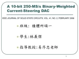
A 10-bit 250-MS/s Binary-Weighted Current-Steering DAC. 班級 : 積體所碩一 學生 : 林義傑 指導教授 : 易序忠老師. IEEE JOURNAL OF SOLID-STATE CIRCUITS, VOL. 41, NO. 2, FEBRUARY 2006. Outline. Proposed Digital to Analog Converter Simulation Layout Measurement Results. 設計規格. 1. 解析度 (resolution) 為 12bit 。

E N D
A 10-bit 250-MS/s Binary-WeightedCurrent-Steering DAC • 班級: 積體所碩一 • 學生:林義傑 • 指導教授:易序忠老師 IEEE JOURNAL OF SOLID-STATE CIRCUITS, VOL. 41, NO. 2, FEBRUARY 2006
Outline • Proposed Digital to Analog Converter • Simulation • Layout • Measurement Results
設計規格 1. 解析度 (resolution)為12bit。 2. 差動非線性誤差(Differential Nonlinearity Error DNL)小於0.5 ILSB 3. 累積非線性誤差(Integral Nonlinearity Error INL) 小於0.5 ILSB。 4. 轉換率 (Conversion Rate ) 100MS/S。 5. 功率損耗 (Power Dissipation) 100mW。 6. 電源電壓3.3V。 7. 使用製程 為tsmc 0.35um 2p4m。 8. 晶片面積為3.3 mm2。
12-bit 數位/類比轉換器電路架構 兩級式切換電流源數位/類比轉換器
差動式切換開關驅動控制電路 Vin+ Vin-
增加電流源輸出阻抗技術 可抑制開關動作所造成地電荷回饋到電 流源,減少輸出端電壓波動對電流源影響,以增加電流源穩定,同時也使輸出端電壓範圍增大。
電流源梯度誤差 • 在數位轉類比電路中,電流源的準確性受到製程影 響,其中除了Vth的變異外尚有電晶體寬(W) 和長(L) 因為光罩所造成的誤差,閘極氧化層厚度(tox)因為加 溫氧化時間不同或是溫度不均勻等,均會影響閘極氧 化層的厚度,及封裝後受應力不同⋯等也都會造成影響。
降低電流源梯度誤差 四象限對稱配置
栓鎖電路 栓鎖電路
電流源設計規格 高六位元採用二進位碼轉換溫度計碼採用四象限對稱佈局,因此 在溫度計碼控制部份電流源為表上最大W/L 的四倍,也就是在實 際電路上有效MSB 的電晶體規格為(W/L)P=(8/2)*4(um),而二進 位碼控制部份最大電流源電晶體規格為(W/L)P=(8/2)*2 (um), 次大者電晶體規格為(W/L)P=(8/2)*1 (um)