Download
1 / 7
70 likes | 622 Views
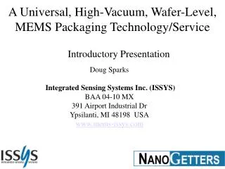
A Universal, High-Vacuum, Wafer-Level, MEMS Packaging Technology/Service. Introductory Presentation. Doug Sparks Integrated Sensing Systems Inc. (ISSYS) BAA 04-10 MX 391 Airport Industrial Dr Ypsilanti, MI 48198 USA www.mems-issys.com. MEMS Vacuum Packaging.

E N D
A Universal, High-Vacuum, Wafer-Level, MEMS Packaging Technology/Service Introductory Presentation Doug Sparks Integrated Sensing Systems Inc. (ISSYS) BAA 04-10 MX 391 Airport Industrial Dr Ypsilanti, MI 48198 USA www.mems-issys.com
MEMS Vacuum Packaging Vacuum packaging is used for many MEMS devices: gyroscopes, RF-MEMS, optical displays, IR sensors, density meters, resonant clocks, Coriolis mass flow sensors, vacuum microelectronics, density meters, pressure sensors… Vacuum sealing can be accomplished at the package level (metal or ceramic packages) or at the chip/wafer level.
NanoGetter Thin-Film Technology To improve the vacuum quality of ISSYS resonant sensors, reduce particle contamination and simplify the processing, a new gettering technology, called NanoGetters due to the very thin metal layers employed, was developed. NanoGettersTM are covered by pending patents and US patent 6,499,354
The process flow for glass frit wafer bonding, including the addition of the thin film getter used to form the chip-level vacuum package. NanoGetter and the Glass Frit Wafer Bonding Process
NanoGetter Patterning & Sealing NanoGetters can be patterned using shadow masking, and various types of standard photolithography techniques. The patterning method depends on the MEMS wafer surface topography and dimensional control requirements. This thin film getter approach can be used with glass frit, eutectic, fusion / silicon direct, anodic and solder bonding
Vacuum Performance – High Q ResonatorsUsing the NanoGetter Process/Design Q=61,700 Q values of 2,000-68,000 are obtained by wafer-level vacuum packaging With No Nanogetter – the average Q value is 36, standard deviation=17
Program Goals & Status 7/04-7/05 • Optimize the getter formulation and deposition process -Done • Conduct reliability tests on the optimized getter - Done • Standardize the design guidelines and processes for integrating the getter into the various wafer-level vacuum sealing technologies for 100mm-150mm wafer diameters – On-Going • Insert the new design guidelines into MEMS Exchange – On-Going • Integrate and run getters for initial DoD customers.