Download
1 / 19
200 likes | 406 Views
Origin of Coulomb Blockade Oscillations in Single-Electron Transistors Fabricated with Granulated Cr/Cr 2 O 3 Resistive Microstrips. Xiangning Luo, Alexei O. Orlov, and Gregory L. Snider University of Notre Dame, Dept. of Electrical Engineering, Notre Dame, IN 46556. Outline.

E N D
Origin of Coulomb Blockade Oscillations in Single-Electron Transistors Fabricated with Granulated Cr/Cr2O3 Resistive Microstrips Xiangning Luo, Alexei O. Orlov, and Gregory L. Snider University of Notre Dame, Dept. of Electrical Engineering, Notre Dame, IN 46556
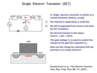
Outline • Purpose: to understand single-electron devices with resistive microstrips instead of tunnel junctions • Can single-electron transistor be built using only resistors with no tunnel junctions? • SETs with metal islands and resistive microstrips are fabricated and tested. Coulomb blockade oscillations are observed, but what is the origin of these oscillations? • Possible mechanisms for Coulomb blockade oscillations are investigated and discussed
Fabrication of CrOx SETs by Two Steps of E-beam Lithography and Deposition • Why two steps? To eliminate junctions! • First layer e-beam lithography and metal deposition define the Au electrodes and island (2 nm Ti and 10 nm Au) • The CrOx resistive microstrips connecting the island to the electrodes are formed in the second e-beam lithography and deposition step. • Cr (8 nm-10 nm or 40 nm) was evaporated in the oxygen ambient. By controlling the oxygen pressure and deposition rate, different values of sheet resistance of CrOx film were achieved.
Au Cr Different Contact Designs (Type #1) Gate Gate Cr Au SiO2 Island Island Drain Cr Source Drain Cr Cr Source Cr Type #1: large tabs (wider than 300nm in two dimensions) on both ends cover all of the steps where the two layers of metal overlap.
Measurements on type #1 (tabs everywhere) SETs • Over 95% devices showed conductance at room temperature. • The CrOx films were very uniform and lasted for a long time when exposed to air. • In the low temperature measurement (300mK) • R<2 kΩ/□, weak temperature dependence • 2 kΩ /□<R<7 kΩ /□, significant nonlinearities and a temperature dependence characteristic of variable range hopping were observed; however, none of the devices exhibited Coulomb blockade oscillations. • R>7 kΩ /□, all of the devices were frozen out, showing no conductivity below 5 KΩ.
Different Contact Designs (Type #2) Gate Gate Au Cr Cr Au SiO2 Island Island Drain Source Drain Cr Cr Cr Source Cr Type #2: large tabs only cover the steps of source and drain and no tabs appear on the island.
Measurements on type #2 SETs Coulomb blockade oscillations were only observed in devices with NARROW LINES touching the island The yield vs. resistance of type #2 devices • Coulomb blockade oscillations were only observed when the resistance of devices was greater than 100 k Ω. • Devices with higher resistance were more likely to show Coulomb blockade oscillations
Low Temperature Measurements (Type#2) (b) (a) (a) I-V curves of an SET in open state and blocked state. (b) I-Vg modulation curve of the same SET of (a) measured at 300 mK showed deep modulation by the gate.
Low Temperature Measurements (Type#2) Charging diagram of an SET measured at 300 mK showed a charging energy of ~ 0.4 meV.
AFM Images (a) (b) Gate Au island CrOx wire with tabs CrOx wire Large tab Au island • AFM image of a CrOx wire deposited on the edge of Au island. • The AFM image of an abnormal SET revealed that only two edges were covered by large tabs in the sample with a pattern shift.
Step Edge Junctions or Resistive microstrips with “right” resistance and capacitance? (b) Au island Cr SiO2 Au (a) Au island Cr Cr (c) Au island Cr SiO2 R>RQ C « e2/2kBT Top view (a), cross section (b) of step edge junction, the areas where step edge junctions formed are marked by circles, and cross section (c) showing resistive microstrips with “right” resistance and capacitance.
AFM Image Island Gate CrOx Gate Au layer The abnormal devices which had a very rough surface of CrOx films.
Multiple Frequencies in I-Vg Modulation Curves Multiple frequencies in I-Vg modulation curve of abnormal devices with a very rough CrOx surface.
SETs with Thicker CrOx Wires (Type #2) • SETs with thicker (~ 40 nm) CrOx wires were also fabricated using pattern design type #2 with different widths of island (80 nm and 500 nm). • The room temperature sheet resistance of the devices showing significant nonlinearity in I-V curves at 300 mK is around 5 kΩ/□, which is about the same as our previous SETs with thinner (8-10nm) CrOx wires. • Among those devices having significant nonlinearity, about 95% (21 out of 22) exhibited Coulomb blockade oscillations, which is much higher than that of SETs with thinner CrOx wires. • Tunnel barriers other than step edge junction formed at the interface of Au island and CrOx providing small enough capacitance and resistance lager than RQ to fulfilled the two requirements of Coulomb blockade oscillations
Low Temperature Measurements SETs with Thicker CrOx Wires (Type #2) (b) (a) (a) I-Vg modulation curves of an SET with 40 nm thick CrOx strips showed deep modulation by the gate. (b) Charging diagram of the same SET of (a) measured at 12 mK
Low Temperature Measurements SETs with Thicker CrOx Wires (Type #2) Temperature dependence of an SET with thicker CrOx wires
Low Temperature Measurements of a CrOx Wire Crossed Over Two Au wires Au Gate Cr Source Drain (a) Schematic of the layer of a CrOx wire crossed over two Au wires. (b) Coulomb blockade oscillations observed on this structure at 300 mK.
SETs with Pt as the First Layer • SETs with Pt instead of Au as the first layer and thicker (~ 40 nm) CrOx as the second layer were also fabricated using pattern design type #3. • Most of the devices showed significant nonlinearity in I-V curves at 300 mK. • None of these devices showed any gate dependence. • More experiments are needed.
Conclusions • Two basic requirements to observe single electron tunneling effects: • the total capacitance of the island, C, must be small enough that the charging energy EC = e2/2C >> kBT. • the resistance of the tunnel barriers, RT > RQ = 25.8 k to suppress quantum charge fluctuations. • Resistive microstrip itself does not provide localization of electrons in the island - first requirement may not be fulfilled. • Two possible explanations: • Step edge “break junctions” with low C are formed at the connecting interface between CrOx wires and Au wires • Microstrips with small overlapping area and high resistance may satisfy both requirements