Download
1 / 23
820 likes | 1.89k Views
Abstract: HEMT is a field effect transistor incorporating a junction between two materials with different band gaps as the channel. We will discuss different types of HEMTs and their Applications. High Electron Mobility Transistors.

E N D
Abstract: HEMT is a field effect transistor incorporating a junction between two materials with different band gaps as the channel. We will discuss different types of HEMTs and their Applications. High Electron Mobility Transistors Presented by: Date: 04/28/2014 SujanaKorrapati, SaiDivya Anne
Outline • Introduction • GaN HEMT structure and operation principles • Design rules for AlGaN/GaN HEMT • InP HEMT • Comparison of GaN HEMT with GaAs HEMT • Applications in Technology • Summary
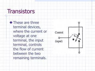
Introduction • Transistors are used in electronic devices e.g. switch, amplifiers, oscillators • To satisfy the growing demands of • High Power • High Speed • High Efficiency communications • Conventional HEMTs use a AlGaAs/GaAsAlGaN/GaN
Basic GaN HEMT Structure Source: http://www.eetimes.com/document.asp?doc_id=1272514
Gallium Nitrate • High electron density(Polarization effects) • Adequate for high power amplifiers High Breakdown voltage • Large heat capacity • Necessary to growth in a wafer of another material • Molecular Beam Epitaxy • Metal Organic Vapor Beam Epitaxy
Substrate Material • Sapphire • Most used material, cheap, good quality commercial wafers. • Poor thermal conductivity. • Silicon Carbide • Low lattice mismatch. • High thermal capacity. • Silicon • Most common semiconductor. • Acceptable thermal conductivity.
Operation principles (Polarization) AlGaN/GaN HEMTs transistor don’t need doping to obtain a high electron density. Spontaneous polarization. + Piezoelectronic polarization. = 1013 (cm2/Vs) carrier concentration
Enegry Band Diagram of GaN/AlGaN HEMT • HEMTs utilize heterojunction between two semiconducting materials to confine electrons to a triangular quantum well. • Conduction band edge EC and Fermi level EF determine the electron density in the 2DEG Source:http://research.pbsci.ucsc.edu/chemistry/li/research.html
Heterojunction • Heterojunction: 2 layers • Highlydoped layer with grand gap • Non-doped layer withsmall gap
Design Rules ForGaN/AlGaN HEMTs:Materials Perspective • Thickness of the Barrier Layer • Al composition of the barrier layer • Nucleation and Buffer layer • Substrate for epitaxial growth
Design Rules ForGaN/AlGaN HEMTs:Fabrication Perspective • Gate footprint, cross-sectionalarea andwidthcontrols thefrequency response • Gate drain spacingaswellasgatefootprintdeterminesthebreakdownvoltage • Geometryofthedevice alsoplaysarole
InP HEMT Source: http://www.mwe.ee.ethz.ch/en/about-mwe-group/research/vision-and-aim/high-electron-mobility-transistors-hemt.html
Advantages of InP based HFETs • Lower noise • Higher cutoff frequency • Higher gain • Operating voltage below 3 V
Comparison of GaN HEMT with GaAs HEMT ΦB GaN AlGaN Ec ∆Ec EF d AlGaAs donor σcomp σB +ve GaAs buffer layer 2 DEG σsurf AlGaAsspacer AlGaN/GaN HEMT AlGaAs/GaAsHEMT
HEMT Applications • A Monolithic HEMT Passive Switch for Phased- Array Applications • High Power and High Efficiency GaN-HEMT for Microwave Communication Applications • Highly efficient high power InP HEMT amplifiers for high frequency applications • Highly Uniform InAlAs–InGaAs HEMT Technology for High-Speed Optical Communication System ICs
A Monolithic HEMT Passive Switch for Phased- Array Applications A 0.2 x 200 ,um2 HEMT device is used as a series passive FET switch
High Power and High Efficiency GaN-HEMT for Microwave Communication Applications In the typical mobile communication band of more than 2GHz, the RF signal loss through the Cds and Rs becomes significant. Thus, the minimization of Cds is effective in the high efficiency amplification.
InAlAs–InGaAs HEMT Technology for High-Speed Optical Communication System ICs • Uniformity of the transistors is required to fabricate high-speed ICs • ICs with more than 1000 transistors were fabricated using Y-shaped gate technology and operated at 40 Gb/s
Summary & Conclusions • HEMT transistor are widely used in electronic application • AlGaN/GaN structure looks promising • AlGaN/GaN HEMT grown on Si substrate not only reduces the production cost but also prepares for the possible combination of GaN devices and Si technology
References • http://ieeexplore.ieee.org/stamp/stamp.jsp?tp=&arnumber=536950 • http://ieeexplore.ieee.org/stamp/stamp.jsp?tp=&arnumber=5877127 • http://ieeexplore.ieee.org/stamp/stamp.jsp?tp=&arnumber=1219481 • “Characterization of advanced AlGaN HEMT structures” Anders Lundskog. • http://ieeexplore.ieee.org/stamp/stamp.jsp?tp=&arnumber=877122
Five Key Points about HEMT • 3 contacts: Source and drain ohmic contacts. GateSchottky barrier • Conventional HEMTs use a AlGaAs/GaAsAlGaN/GaN • High electron density (Polarization effects) • The HEMT-HBT monolithic microwave integrated circuit (MMIC) is fabricated using selective molecular beam epitaxy (MBE) • InAlAs-InGaAs HEMT grown on InP substrate promises excellent gain and noise performance for amplifier applications