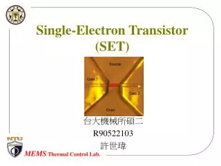
Single Electron Transistors (SET)
Single Electron Transistors (SET). EE 240 Group 6 05-06-05 Adit Gupta, Sandeep Kotak, Ana MartinezMarrosu, Erik Stegall. Overview:. Summary Background Creation Formulas Problems Devices and Applications Future/Closing. Introduction:. Summary: Definition:

Single Electron Transistors (SET)
E N D
Presentation Transcript
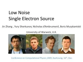
Single Electron Transistors (SET) EE 240 Group 6 05-06-05 Adit Gupta, Sandeep Kotak, Ana MartinezMarrosu, Erik Stegall
Overview: • Summary • Background • Creation • Formulas • Problems • Devices and Applications • Future/Closing
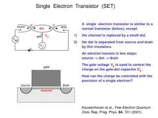
Introduction: Summary: Definition: An ultra-small device, that transfers one electron at a time, based on Coulomb interaction. This occurs on a tiny conducting layer know as an island. This island’s electrostatic potential increases significantly with the introduction of just one electron. Single-electron transistors SET's are considered to be the elements of the future. In this future, integrated circuits will be highly dense and low powered. These ultra-low powered circuits will be of a nanometer scale electronic and they will be able to detect the motion of individual electrons. Problems, however, are that SET's have low voltage gain, high output impedances, and are sensitive to random background charges. Also, for SET’s to be useful in practical applications they must be able to operate in room temperature. SETs are required to be no larger than ~10 nm. This is why its highly unlikely that single-electron transistors would ever replace field-effect transistors (FET's) which work better in applications where large voltage gain or low output impedance is necessary.
Background: The start of the SET transistor began in 1985 thanks to Dmitri Averin and Konstantin Likharev. They proposed the idea of a new three-terminal device called a single-electron tunneling (SET) transistor. Two years later Theodore Fulton and Gerald Dolan at Bell Labs in the US, created such a device and demonstrated how it would operate. • What are SET transistor made from: • Single-electron transistors have been made with just a few nanometers using; • Metals • Semiconductors • Carbon nanotubes • Individual molecules. [5-7] The charging of electrons for a tunnel junction with an Capacitance C and an Charge Q has been the bases for how SETs would function. The electric current. I=ΔQ/ Δt, that is associated with tunneling of single electrons is I≈e/τ≥ e^3/2πhC Dmitri Averin, currently a professor at Suny Stony Brook.
Background: General Information about SET Transistors. A single-electron transistor consists of a small conducting island connected to an source and drain leads by tunnel junctions and connected to one or more gates. Generally two gates are used, one used as an input for the SET while the second is used to tune the background charge, a common obstacle needed to be overcome. There are still several problems, to be discussed later, that have slowed the main stream use of SETs. The two more common versions of the 4 stated before are the metallic and semiconductor versions. Coulomb Blockade ->
Creation: Procedure: For Metallic: The first metallic version created by Fulton and Dolan, a material such as a thin aluminum film is used to make all of the electrodes. Beginning with metal being evaporated through a shadow mask that will form the source, drain and gate electrodes. Next the tunnel junctions are formed by adding oxygen to chamber so the metal becomes coated by a thin layer of its natural oxide. Finally, a second layer of the metal, that is shifted from the first by rotating the sample, is evaporated to form the island. For semiconductors: the source, drain and island are obtained by "cutting" regions in a two-dimensional electron gas formed at the interface between two layers of semiconductors such as gallium aluminum arsenide and gallium arsenide. The conducting regions have metallic electrodes patterned on the top semiconductor layer. Negative voltages applied to these electrodes deplete the electron gas just beneath them, and the depleted regions can be made sufficiently narrow to allow tunneling between the source, island and drain. Electrodes that shape the islands can be used as the gate electrode.
Creation: Another way to form an SET is using a scanning tunneling microscope (STM) which can avoid the control problems in self- organized structures. Using this technique an SET can be created that operates at room temperature, showing a clear Coulomb staircase with a ~150 mV period at 300 K. The Process: A 3 nm titanium (Ti) metal film is deposited on a 100 nm thermally oxidized SiO2/n-Si substrate. The Ti surface is oxidized by through the water on the surface via the atmosphere. By using the STM tip as a cathode nanometer size Ti oxide (TiOx) lines can be formed. The barrier height of a TiOx/Ti junction has been found to be 285 meV for the electron from the temperature dependence of the current. Picture of an titanium SET-> Picture of SET using an ATM.
Formulas: Formula for calculating voltage in an island. For n electrons. V(n) = (-ne + Q0 + C1V1 + C2V2 + Cg1Vg1 +Cg2Vg2)/CΣ. The charging energy, Ec = e^2/(2C), sets the energy scale for single-electron effects. The charging energy is typically in the range 1 - 100 meV. A single electron passing through a junction has a change in electrostatic energy = ΔEc =-e(2Q-e)/2C Quantum Conductance Go≡e^2/h Wc = e^2/2C>>KbT when this true the electron is blocked, called Coulomb blockade, when not true electrons can be travel through the junction. Rt >> h/e^2=25.8 kΩ tunneling resistance must be greater then resistance quantum along with the a charged electron energy is greater than the thermal energy is required for tunneling to occur. Polarization charge Qt/Ct+ Qg/Cg= Vg, Qt is polarization charge of tunnel junction and Qg is the gates. 1/(Cs+Cg)*(-ne+e/2_CgVg) > Vd > 1/(Cs+Cg)*(-ne-e/2+CgVg) using Thevenim’s theorem. Used for the relationship of the drain voltage Vd and the gate voltage Vg. Using Thevenim’s theorem in a circuit. • Is a picture of a circuit connected to a source, • Is a picture of a circuit connected to a drain.
Problems: Limiting factors: Most SETs with functional uses need to be at extremely low temperatures around 100 mK. Background charge problem, is an issue that is the greatest inhibiter of the widespread use of SET's. The cause of the background charge problem is the extreme charge sensitivity of SET's. A single charged vacancy or an ion in the oxide layers near a SET can be enough to switch the transistor from the being conducting to being non-conducting. Voltage gain decreases as the size of the device decreases, because voltage decreasing with gate capacitance. This requires an extra volts having to be applied to an output of a few mV. But there is a limit to the voltage increase and it is connected to gate capacitance. The voltage increases until the charging energy is of order kbT, then it drops. This graph shows that it is very difficult make SETs with voltages greater than those that operate at room temperature. This is even harder for dense integrated circuits that operate at 400 K.
Device & App: • Radio-Frequency SET - fast-response and high-sensitivity electrometer RF-SET has the sensitivity and speed to count electrons at frequencies >10 MHz (that is, measure a current on the order of pico-amperes, electron by electron) where the 1/f noise due to background charge motion is completely negligible. • Applications of the RF-SET • Fast and accurate counting of electrons on nanosecond time scales, for electrical metrology. • Detection and analysis of charge Qubit imperfections. • Directly probing the Hamiltonian of high impedance electrical circuits, such as molecular nanowires, through ultra-sensitive polarized measurements. 500 nm A comparison of the performance of different SET and conventional memory technologies
Applications: • SETs used toincrease battery life in portable electronics: • Blick's transistor: the "island" is connected to a tiny nanopillar that oscillates. • This new mechanical model can operate at room temperature. • This research will result in smaller and less power-greedy electronic items • Single-Electron MOS Memory (SEMM) • Coulomb Blockade • Miniature Flash Memory • Yano Type Memory
Solutions: Currently the best way to use SETs is in an hybrid setting. Mostcommonly is that of an FET/SET combination. FETs would be used to speed the charge measurement and should be placed as close as possible to the SET. The FET can also buffer the high output impedance produced by the SET. While this method weakens the case for all SET circuits, it at least provides a building block and provides a more efficient way to use circuits with FETs. • Is a picture of a charged lock loop that will automatically tune away background charge. • Is a schematic of an SET with an FET output stage with a voltage graph, solid that of the SET, dotted of the FET
The Future, Logic and Electrometers: SETMOS: Using a hybrid combination, similar to that of SET and FET, of SETs and CMOS transistors in SETMOS devices can provide enough gain and current drive to perform logic functions on a much smaller scale than possible with just an CMOS. The SETMOS device exhibits Coulomb blockade oscillations similar to a traditional SET but offers much higher current-driving capability. Similar to a CMOS this SETMOS uses a single electron to represent an logic state. It works on the notation of Coulomb Blockade oscillations, but operates at a much faster current-driving capability. What’s to come, “quantum” computers.
The Future: More uses of electrometers Electrometers based on SET transistors could also be used to measure the quantum superposition of charge states in a island connected by a tunnel junction to a superconductor. Islands could therefore provide a means for implementing the quantum bits needed for a quantum computer. Professor Daniel Prober and Professor Robert Schoelkopf from the Department of Applied Physics at Yale, have created an ultra fast, single-electron transistor which could lead to the development of "quantum" computers with supercomputer powers and the size of a thumbtack. The breakthrough involves inducing a small part of the transistor that will "resonate" with the arrival of each electron. This resonance creates a way for tracking each electron and also gives an extra bit of energy to push the electrons as they are moving through the switch, this makes it 1,000 times faster than any previous device.
Work Cited: • Stevenson T. R, Pellerano F.A, Stahle C.M, Aidala K, Schoelkopf R.J. 2002, • Applied Physics Letters, 80, 16. • Bladh K, Gunnarsson D, Johansson G, Käck A, wendin G, Delsing P, Aassime A, • Taslakov M. “Reading out Charge Qubits with a Radio Frequency Single Electron • Transistor“, 2002. • Berman D, Zhitenev N. B, Ashoori R.C, Smith H, Melloch M, 1997, American • Vacuum Society, 2844. • Schoelopf R. J, Wahlgren P, Kozhevnikov A, Delsing P, Prober D. 1998, Science, • 280, 1238. • http://www.princeton.edu/~chouweb/newproject/research/SEM/SelfLimitChargProc.html • Guo L, Leobandung E, Chou S. Y. 1997, Science, 275, 649. • http://homepages.cae.wisc.edu/~wiscengr/feb05/transitioningelecfrontiers.shtml • Paul D. J, “Nanoelectronics”, University of Cambridge, CB3 0HE, UK.
And…Scene Don't Worry, You have Questions We have Answers