Lecture 8. Memory Hierarchy Design I
640 likes | 812 Views
COM515 Advanced Computer Architecture. Lecture 8. Memory Hierarchy Design I. Prof. Taeweon Suh Computer Science Education Korea University. CPU vs Memory Performance. µProc 55%/year (2X/1.5yr). Moore’s Law. The performance gap grows 50%/year. DRAM 7%/year (2X/10yrs).

Lecture 8. Memory Hierarchy Design I
E N D
Presentation Transcript
COM515 Advanced Computer Architecture Lecture 8. Memory Hierarchy Design I Prof. Taeweon Suh Computer Science Education Korea University
CPU vs Memory Performance µProc 55%/year (2X/1.5yr) Moore’s Law The performance gapgrows 50%/year DRAM 7%/year (2X/10yrs) Prof. Sean Lee’s Slide
I/O, Memory, Cache CPU An Unbalanced System Source: Bob Colwell keynote ISCA’29 2002 Prof. Sean Lee’s Slide
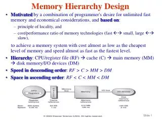
Memory Issues • Latency • Time to move through the longest circuit path (from the start of request to the response) • Bandwidth • Number of bits transported at one time • Capacity • Size of memory • Energy • Cost of accessing memory (to read and write) Prof. Sean Lee’s Slide
Model of Memory Hierarchy SRAM DISK DRAM Main Memory Reg File L1 Data cache L2 Cache L1 Inst cache Slide from Prof Sean Lee in Georgia Tech
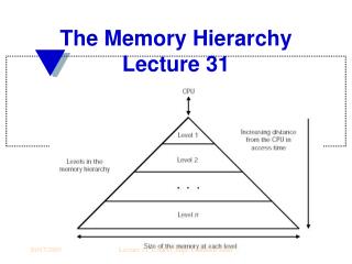
Levels of Memory Hierarchy Upper Level Capacity Access Time Cost Staging Transfer Unit faster Registers CPU Registers 100s Bytes <10 ns Compiler 1-8 bytes Instr. Operands Cache K Bytes (Now, MB) 10-100 ns 1-0.1 cents/bit Cache Cache controller 8-128 bytes Cache Lines Main Memory M Bytes (Now, GB) 200ns- 500ns $.0001-.00001 cents /bit Memory Operating system 512-4K bytes Pages Disk G Bytes, 10 ms (10,000,000 ns) 10-5 - 10-6 cents/bit Disk larger Lower Level Modified from the Prof Sean Lee’s slide in Georgia Tech
Topics covered • Why do caches work • Principle of program locality • Cache hierarchy • Average memory access time (AMAT) • Types of caches • Direct mapped • Set-associative • Fully associative • Cache policies • Write back vs. write through • Write allocate vs. No write allocate Prof. Sean Lee’s Slide
Why Caches Work? • The size of cache is tiny compared to main memory • How to make sure that the data CPU is going to access is in caches? • Caches take advantage of the principle of locality in your program • Temporal Locality (locality in time) • If a memory location is referenced, then it will tend to be referenced again soon. So, keep most recently accessed data items closer to the processor • Spatial Locality (locality in space) • If a memory location is referenced, the locations with nearby addresses will tend to be referenced soon. So, move blocks consisting of contiguous words closer to the processor
D C[99] C[98] C[97] C[96] . . . . . . . . . . . . . . C[7] C[6] C[5] C[4] C[3] C[2] C[1] C[0] . . . . . . . . . . . . . . B[11] B[10] B[9] B[8] B[7] B[6] B[5] B[4] B[3] B[2] B[1] B[0] A[99] A[98] A[97] A[96] . . . . . . . . . . . . . . A[7] A[6] A[5] A[4] A[3] A[2] A[1] A[0] Example of Locality int A[100], B[100],C[100],D; for (i=0; i<100; i++) { C[i] = A[i] * B[i] + D; } Cache A Cache Line (block) Slide from Prof Sean Lee in Georgia Tech
A Typical Memory Hierarchy • Take advantage of the principle of locality to present the user with as much memory as is available in the cheapest technology at the speed offered by the fastest technology lower level higher level Secondary Storage (Disk) On-Chip Components Main Memory (DRAM) CPU Core L2 (Second Level) Cache L1I (Instr Cache) ITLB Reg File L1D (Data Cache) DTLB Speed (cycles): ½’s 1’s 10’s 100’s 10,000’s Size (bytes): 100’s 10K’s M’s G’s T’s Cost: highest lowest
A Computer System Caches are located inside a processor Processor Main Memory (DDR2) FSB (Front-Side Bus) North Bridge Graphics card DMI (Direct Media I/F) South Bridge Hard disk USB PCIe card
DL1 DL1 Core0 Core1 IL1 IL1 L2 Cache Core 2 Duo (Intel) Source: http://www.sandpile.org
Core i7 (Intel) • 4 cores on one chip • Three levels of caches (L1, L2, L3) on chip • L1: 32KB, 8-way • L2: 256KB, 8-way • L3: 8MB, 16-way • 731 million transistors in 263 mm2 with 45nm technology
Opteron (AMD) - Barcelona • 4 cores on one chip • Three levels of caches (L1, L2, L3) on chip • L1: 64KB, L2: 512KB, L3: 2MB • Integrated North Bridge
Core i7 (2nd Gen.) 2nd Generation Core i7 Sandy Bridge 995 million transistors in 216 mm2 with 32nm technology
Intel Itanium 2 (2002~) 3MB Version 180nm 421 mm2 6MB Version 130nm 374 mm2 Prof. Sean Lee’s Slide
Core 0 Core 0 3MB 3MB 3MB 3MB Core 1 3MB 3MB 3MB 3MB Xeon Nehalem-EX (2010) • 24MB Shared L3 Modified from Prof. Sean Lee’s Slide
Example : STI Cell Processor Local Storage SPE = 21M transistors (14M array; 7M logic) Prof. Sean Lee’s Slide
Cell Synergistic Processing Element Each SPE contains 128 x128 bit registers, 256KB, 1-port, ECC-protected local SRAM (Not cache) Prof. Sean Lee’s Slide
Cache Terminology • Hit: data appears in some block • Hit Rate: the fraction of memory accesses found in the level • Hit Time: Time to access the level (consists of cache access time + time to determine hit) • Miss: data needs to be retrieved from a block in the lower level (e.g., Block Y) • Miss Rate= 1 - (Hit Rate) • Miss Penalty: Time to replace a block in the upper level + Time to deliver the block to the processor • Hit Time << Miss Penalty Lower Level Memory Upper Level Memory From Processor Blk X Blk Y To Processor
Average Memory Access Time • Average memory-access time = Hit time + Miss rate x Miss penalty • Miss penalty: time to fetch a block from lower memory level • access time: function of latency • transfer time: function of bandwidth b/w levels • Transfer “one block (one cache line)” at a time • Transfer at the size of the memory-bus width
Main Memory (DRAM) First-level Cache Memory Hierarchy Performance 1 clk 300 clks Miss % * Miss penalty Hit Time • Average Memory Access Time (AMAT) = Hit Time + Miss rate * Miss Penalty = Thit(L1) + Miss%(L1) * T(memory) • Example: • Cache Hit = 1 cycle • Miss rate = 10% = 0.1 • Miss penalty = 300 cycles • AMAT = 1 + 0.1 * 300 = 31 cycles • Can we improve it?
Third Level Cache Second Level Cache Main Memory (DRAM) First-level Cache Reducing Penalty: Multi-Level Cache 1 clk 10 clks 20 clks 300 clks L1 L2 L3 On-die Average Memory Access Time (AMAT) = Thit(L1) + Miss%(L1)* (Thit(L2) + Miss%(L2)* (Thit(L3) + Miss%(L3)*T(memory) ))
AMAT of multi-level memory = Thit(L1) + Miss%(L1)* Tmiss(L1) = Thit(L1) + Miss%(L1)* { Thit(L2) + Miss%(L2)* Tmiss(L2) } = Thit(L1) + Miss%(L1)* { Thit(L2) + Miss%(L2) * [ Thit(L3) + Miss%(L3) * T(memory) ] }
AMAT Example AMAT = Thit(L1) + Miss%(L1)* (Thit(L2) + Miss%(L2)* (Thit(L3) + Miss%(L3)*T(memory) ) ) • Example: • Miss rate L1=10%, Thit(L1) = 1 cycle • Miss rate L2=5%, Thit(L2) = 10 cycles • Miss rate L3=1%, Thit(L3) = 20 cycles • T(memory) = 300 cycles • AMAT = ? • 2.115 (compare to 31 with no multi-levels) 14.7x speed-up!
Types of Caches • DM and FA can be thought as special cases of SA • DM 1-way SA • FA All-way SA
0x0F 00000 00000 0x55 11111 0xAA 0xF0 11111 Direct Mapping Index Tag Data 0 00000 0 0x55 0x0F 1 00000 00000 1 00001 0 Direct mapping: A memory value can only be placed at a single corresponding location in the cache 11111 0 0xAA 0xF0 11111 11111 1
Set Associative Mapping (2-Way) Index Data Tag Way 0 Way 1 0 0000 0 0x55 0000 0 0 0x55 0x0F 0x0F 1 0000 1 1 0000 1 0 Set-associative mapping: A memory value can be placed in any location of a set in the cache 1111 0 0 0xAA 1111 0 0xAA 0xF0 0xF0 1111 1 1 1111 1
0x0F 0x0F 0000 0000 0000 0000 0x55 0x55 1111 1111 0xAA 0xAA 0xF0 0xF0 1111 1111 000000 0x55 0x0F 000001 000110 111110 0xAA 0xF0 111111 Fully Associative Mapping Tag Data 000000 0x55 0x0F 000001 000110 Fully-associative mapping: A memory value can be placed anywhere in the cache 111110 0xAA 0xF0 111111
Direct Mapped Cache Memory Address • Cache location 0 is occupied by data from: • Memory locations 0, 4, 8, and C • Which one should we place in the cache? • How can we tell which one is in the cache? DM Cache 0 1 Cache Index 2 0 3 1 4 2 5 3 6 7 A Cache Line (or Block) 8 9 A B C D E F
Three (or Four) Cs (Cache Miss Terms) • Compulsory Misses: • cold start misses (Caches do not have valid data at the start of the program) • Capacity Misses: • Increase cache size • Conflict Misses: • Increase cache size and/or associativity. • Associative caches reduce conflict misses • Coherence Misses: • In multiprocessor systems (later lectures…)
Example: 1KB DM Cache, 32-byte Lines • The lowest M bits are the Offset (Line Size = 2M) • Index = log2 (# of sets) Address 31 9 4 0 Tag Index Offset Ex: 0x01 Ex: 0x00 Valid Bit Cache Tag Cache Data : Byte 31 Byte 1 Byte 0 0 : Byte 63 Byte 33 Byte 32 1 2 3 # of set : : : : Byte 1023 Byte 992 31
Example of Caches • Given a 2MB, direct-mapped physical caches, line size=64bytes • Support up to 52-bit physical address • Tag size? • Now change it to 16-way, Tag size? • How about if it’s fully associative, Tag size?
27 26 25 24 Example: 1KB DM Cache, 32-byte Lines • lw from 0x77FF1C68 Tag Index Offset 77FF1C68 = 0111 0111 1111 1111 0001 1100 0101 1000 Tag array Data array Index=2 DM Cache
DM Cache Speed Advantage • Tag and data access happen in parallel • Faster cache access! Offset Tag Index Tag array Data array Index
Associative Caches Reduce Conflict Misses • Set associative (SA) cache • multiple possible locations in a set • Fully associative (FA) cache • any location in the cache • Hardware and speed overhead • Comparators • Multiplexors • Data selection only after Hit/Miss determination (i.e., after tag comparison)
Cache Data Cache Tag Valid Cache Line 0 : : : Compare Set Associative Cache (2-way) • Cache index selects a “set” from the cache • The two tags in the set are compared in parallel • Data is selected based on the tag result • Additional circuitry as compared to DM caches • Makes SA caches slower to access than DM of comparable size Cache Index Valid Cache Tag Cache Data Cache Line 0 : : : Adr Tag Compare 1 0 Mux Sel1 Sel0 OR Cache Line Hit
Set-Associative Cache (2-way) • 32 bit address • lwfrom 0x77FF1C78 Tag Index offset Tag array0 Data aray0 Data array1 Tag array1
= = = = Fully Associative Cache tag offset Data Tag Associative Search Multiplexor Rotate and Mask
Fully Associative Cache Tag offset Write Data Address Tag Data Tag Data Tag Data Tag Data compare compare compare compare Additional circuitry as compared to DM caches More extensive than SA caches Makes FA caches slower to access than either DM or SA of comparable size Read Data
Cache Write Policy • Write-through -The value is written to both the cache line and to the lower-level memory. • Write-back - The value is written only to the cache line. The modified cache line is written to main memory only when it has to be replaced. • Is the cache line clean (holds the same value as memory) or dirty (holds a different value than memory)?
Write-through Policy 0x1234 0x1234 0x1234 0x5678 0x5678 0x1234 Processor Cache Memory
Write Buffer • Processor: writes data into the cache and the write buffer • Memory controller: writes contents of the buffer to memory • Write buffer is a FIFO structure: • Typically 4 to 8 entries • Desirable: Occurrence of Writes << DRAM write cycles • Memory system designer’s nightmare: • Write buffer saturation (i.e., Writes DRAM write cycles) Cache Processor DRAM Write Buffer Prof. Sean Lee’s Slide
Writeback Policy 0x1234 0x1234 0x1234 0x5678 0x9ABC 0x5678 0x1234 0x5678 Processor Cache Memory
On Write Miss • Write-allocate • The line is allocated on a write miss, followed by the write hit actions above. • Write misses first act like read misses • No write-allocate • Write misses do not interfere cache • Line is only modified in the lower level memory
Quick recap • Processor-memory performance gap • Memory hierarchy exploits program locality to reduce AMAT • Types of Caches • Direct mapped • Set associative • Fully associative • Cache policies • Write through vs. Write back • Write allocate vs. No write allocate Prof. Sean Lee’s Slide
Cache Replacement Policy • Random • Replace a randomly chosen line • FIFO • Replace the oldest line • LRU (Least Recently Used) • Replace the least recently used line • NRU (Not Recently Used) • Replace one of the lines that is not recently used • In Itanium2 L1 Dcache, L2 and L3 caches Prof. Sean Lee’s Slide
E G C C D A E D C C A E D B C B D D A A LRU Policy MRU-1 LRU+1 LRU MRU A B C D Access C Access D Access E MISS, replacement needed Access C MISS, replacement needed Access G Prof. Sean Lee’s Slide
LRU From Hardware Perspective LRU Way3 Way2 Way1 Way0 Access update State machine Access D A B C D LRU policy increases cache access times Additional hardware bits needed for LRU state machine Prof. Sean Lee’s Slide
LRU Algorithms • True LRU • Expensive in terms of speed and hardware • Need to remember the order in which all N lines were last accessed • N! scenarios –O(log N!) O(N log N) LRU bits • 2-ways AB BA = 2 = 2! • 3-ways ABC ACB BAC BCA CAB CBA = 6 = 3! • Pseudo LRU: O(N) • Approximates LRU policy with a binary tree Prof. Sean Lee’s Slide