Download
1 / 61
610 likes | 752 Views
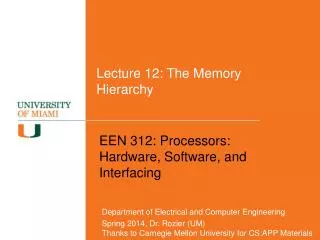
Lecture 12: The Memory Hierarchy. EEN 312: Processors: Hardware, Software, and Interfacing. Department of Electrical and Computer Engineering Spring 2014, Dr. Rozier (UM) Thanks to Carnegie Mellon University for CS:APP Materials. STORAGE TECHNOLOGY. An Example Memory Hierarchy. L0:.

E N D
Lecture 12: The Memory Hierarchy EEN 312: Processors: Hardware, Software, and Interfacing Department of Electrical and Computer Engineering Spring 2014, Dr. Rozier (UM)Thanks to Carnegie Mellon University for CS:APP Materials
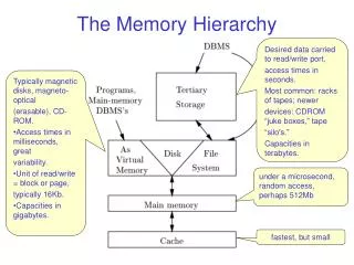
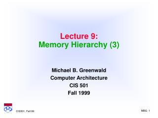
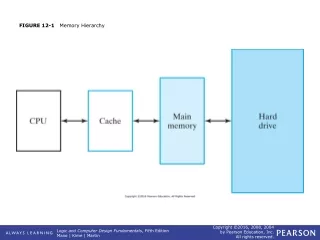
An Example Memory Hierarchy L0: CPU registers hold words retrieved from L1 cache Registers L1: L1 cache (SRAM) L1 cache holds cache lines retrieved from L2 cache Smaller, faster, costlier per byte L2: L2 cache (SRAM) L2 cache holds cache lines retrieved from main memory L3: Main memory (DRAM) Larger, slower, cheaper per byte Main memory holds disk blocks retrieved from local disks Local secondary storage (local disks) L4: Local disks hold files retrieved from disks on remote network servers Remote secondary storage (tapes, distributed file systems, Web servers) L5:
Static RAM (SRAM) 0.5ns – 2.5ns, $2000 – $5000 per GB Dynamic RAM (DRAM) 50ns – 70ns, $20 – $75 per GB Magnetic disk 5ms – 20ms, $0.20 – $2 per GB Ideal memory Access time of SRAM Capacity and cost/GB of disk Memory Technology
Key features RAM is traditionally packaged as a chip. Basic storage unit is normally a cell (one bit per cell). Multiple RAM chips form a memory. Static RAM (SRAM) Each cell stores a bit with a four or six-transistor circuit. Retains value indefinitely, as long as it is kept powered. Relatively insensitive to electrical noise (EMI), radiation, etc. Faster and more expensive than DRAM. Dynamic RAM (DRAM) Each cell stores bit with a capacitor. One transistor is used for access Value must be refreshed every 10-100 ms. More sensitive to disturbances (EMI, radiation,…) than SRAM. Slower and cheaper than SRAM. Random-Access Memory (RAM)
SRAM vs DRAM Summary Trans. Access Needs Needs per bit time refresh? EDC? Cost Applications SRAM 4 or 6 1X No Maybe 100x Cache memories DRAM 1 10X Yes Yes 1X Main memories, frame buffers
d x w DRAM: dw total bits organized as d supercells of size w bits Conventional DRAM Organization 16 x 8 DRAM chip cols 0 1 2 3 Memory controller 0 2 bits / addr 1 rows supercell (2,1) 2 (to/from CPU) 3 8 bits / data Internal row buffer
Step 1(a): Row access strobe (RAS) selects row 2. Step 1(b): Row 2 copied from DRAM array to row buffer. Reading DRAM Supercell (2,1) 16 x 8 DRAM chip Cols 0 Memory controller 1 2 3 RAS = 2 2 / 0 addr 1 Rows 2 3 8 / data Internal row buffer
Step 2(a): Column access strobe (CAS) selects column 1. Step 2(b): Supercell (2,1) copied from buffer to data lines, and eventually back to the CPU. supercell (2,1) supercell (2,1) Reading DRAM Supercell (2,1) 16 x 8 DRAM chip Cols 0 Memory controller 1 2 3 CAS = 1 2 / 0 addr To CPU 1 Rows 2 3 8 / data Internal row buffer
addr (row = i, col = j) bits 56-63 bits 48-55 bits 40-47 bits 32-39 bits 24-31 bits 16-23 bits 8-15 bits 0-7 63 63 56 56 55 55 48 48 47 47 40 40 39 39 32 32 31 31 24 24 23 23 16 16 15 15 8 8 7 7 0 0 64-bit doubleword at main memory address A 64-bit doubleword Memory Modules : supercell (i,j) DRAM 0 64 MB memory module consisting of eight 8Mx8 DRAMs DRAM 7 Memory controller
Basic DRAM cell has not changed since its invention in 1966. Commercialized by Intel in 1970. DRAM cores with better interface logic and faster I/O : Synchronous DRAM (SDRAM) Uses a conventional clock signal instead of asynchronous control Allows reuse of the row addresses (e.g., RAS, CAS, CAS, CAS) Double data-rate synchronous DRAM (DDR SDRAM) Double edge clocking sends two bits per cycle per pin Different types distinguished by size of small prefetch buffer: DDR (2 bits), DDR2 (4 bits), DDR4 (8 bits) By 2010, standard for most server and desktop systems Intel Core i7 supports only DDR3 SDRAM Enhanced DRAMs
DRAM and SRAM are volatile memories Lose information if powered off. Nonvolatile memories retain value even if powered off Read-only memory (ROM): programmed during production Programmable ROM (PROM): can be programmed once Eraseable PROM (EPROM): can be bulk erased (UV, X-Ray) Electrically eraseable PROM (EEPROM): electronic erase capability Flash memory: EEPROMs with partial (sector) erase capability Wears out after about 100,000 erasings. Uses for Nonvolatile Memories Firmware programs stored in a ROM (BIOS, controllers for disks, network cards, graphics accelerators, security subsystems,…) Solid state disks (replace rotating disks in thumb drives, smart phones, mp3 players, tablets, laptops,…) Disk caches Nonvolatile Memories
A bus is a collection of parallel wires that carry address, data, and control signals. Buses are typically shared by multiple devices. Traditional Bus Structure Connecting CPU and Memory CPU chip Register file ALU System bus Memory bus Main memory Bus interface I/O bridge
CPU places address A on the memory bus. Memory Read Transaction (1) Register file Load operation ALU Main memory 0 I/O bridge A Bus interface A x
Main memory reads A from the memory bus, retrieves word x, and places it on the bus. Memory Read Transaction (2) Register file Load operation: ALU Main memory 0 I/O bridge x Bus interface A x
CPU read word x from the bus and copies it into register %eax. Memory Read Transaction (3) Register file Load operation: ALU x Main memory 0 I/O bridge Bus interface A x
CPU places address A on bus. Main memory reads it and waits for the corresponding data word to arrive. Memory Write Transaction (1) Register file Store operation: ALU y Main memory 0 I/O bridge A Bus interface A
CPU places data word y on the bus. Memory Write Transaction (2) Register file Store operation: ALU y Main memory 0 I/O bridge y Bus interface A
Main memory reads data word y from the bus and stores it at address A. Memory Write Transaction (3) register file Store operation: ALU y main memory 0 I/O bridge bus interface A y
What’s Inside A Disk Drive? Spindle Arm Platters Actuator Electronics (including a processor and memory!) SCSI connector Image courtesy of Seagate Technology
Disks consist of platters, each with two surfaces. Each surface consists of concentric rings called tracks. Each track consists of sectors separated by gaps. Disk Geometry Tracks Surface Track k Gaps Spindle Sectors
Aligned tracks form a cylinder. Disk Geometry (Muliple-Platter View) Cylinder k Surface 0 Platter 0 Surface 1 Surface 2 Platter 1 Surface 3 Surface 4 Platter 2 Surface 5 Spindle
Capacity: maximum number of bits that can be stored. Vendors express capacity in units of gigabytes (GB), where1 GB = 109 Bytes (Lawsuit pending! Claims deceptive advertising). Capacity is determined by these technology factors: Recording density (bits/in): number of bits that can be squeezed into a 1 inch segment of a track. Track density (tracks/in): number of tracks that can be squeezed into a 1 inch radial segment. Areal density (bits/in2): product of recording and track density. Modern disks partition tracks into disjoint subsets called recording zones Each track in a zone has the same number of sectors, determined by the circumference of innermost track. Each zone has a different number of sectors/track Disk Capacity
Capacity = (# bytes/sector) x (avg. # sectors/track) x (# tracks/surface) x (# surfaces/platter) x (# platters/disk) Example: 512 bytes/sector 300 sectors/track (on average) 20,000 tracks/surface 2 surfaces/platter 5 platters/disk Capacity = 512 x 300 x 20000 x 2 x 5 = 30,720,000,000 = 30.72 GB Computing Disk Capacity
The read/write head is attached to the end of the arm and flies over the disk surface on a thin cushion of air. By moving radially, the arm can position the read/write head over any track. Disk Operation (Single-Platter View) The disk surface spins at a fixed rotational rate spindle spindle spindle spindle spindle
Disk Operation (Multi-Platter View) Read/write heads move in unison from cylinder to cylinder Arm Spindle
Surface organized into tracks Tracks divided into sectors Disk Structure - top view of single platter
Disk Access Head in position above a track
Disk Access Rotation is counter-clockwise
Disk Access – Read About to read blue sector
Disk Access – Read After BLUEread After reading blue sector
Disk Access – Read After BLUEread Red request scheduled next
Disk Access – Seek After BLUEread Seek for RED Seek to red’s track
Disk Access – Rotational Latency After BLUEread Seek for RED Rotational latency Wait for red sector to rotate around
Disk Access – Read After BLUEread Seek for RED Rotational latency After RED read Complete read of red
Disk Access – Service Time Components After BLUEread Seek for RED Rotational latency After RED read Data transfer Seek Rotational latency Data transfer
Average time to access some target sector approximated by : Taccess = Tavg seek + Tavg rotation + Tavg transfer Seek time (Tavg seek) Time to position heads over cylinder containing target sector. Typical Tavg seek is 3—9 ms Rotational latency (Tavg rotation) Time waiting for first bit of target sector to pass under r/w head. Tavg rotation = 1/2 x 1/RPMs x 60 sec/1 min Typical Tavg rotation = 7200 RPMs Transfer time (Tavg transfer) Time to read the bits in the target sector. Tavg transfer = 1/RPM x 1/(avg # sectors/track) x 60 secs/1 min. Disk Access Time
Given: Rotational rate = 7,200 RPM Average seek time = 9 ms. Avg # sectors/track = 400. Derived: Tavg rotation = 1/2 x (60 secs/7200 RPM) x 1000 ms/sec = 4 ms. Tavg transfer = 60/7200 RPM x 1/400 secs/track x 1000 ms/sec = 0.02 ms Taccess = 9 ms + 4 ms + 0.02 ms Important points: Access time dominated by seek time and rotational latency. First bit in a sector is the most expensive, the rest are free. SRAM access time is about 4 ns/doubleword, DRAM about 60 ns Disk is about 40,000 times slower than SRAM, 2,500 times slower then DRAM. Disk Access Time Example
Modern disks present a simpler abstract view of the complex sector geometry: The set of available sectors is modeled as a sequence of b-sized logical blocks (0, 1, 2, ...) Mapping between logical blocks and actual (physical) sectors Maintained by hardware/firmware device called disk controller. Converts requests for logical blocks into (surface,track,sector) triples. Allows controller to set aside spare cylinders for each zone. Accounts for the difference in “formatted capacity” and “maximum capacity”. Logical Disk Blocks
I/O Bus CPU chip Register file ALU System bus Memory bus Main memory Bus interface I/O bridge I/O bus Expansion slots for other devices such as network adapters. USB controller Graphics adapter Disk controller Mouse Keyboard Monitor Disk
Reading a Disk Sector (1) CPU chip CPU initiates a disk read by writing a command, logical block number, and destination memory address to a port (address) associated with disk controller. Register file ALU Main memory Bus interface I/O bus USB controller Graphics adapter Disk controller keyboard mouse Monitor Disk
Reading a Disk Sector (2) CPU chip Disk controller reads the sector and performs a direct memory access (DMA) transfer into main memory. Register file ALU Main memory Bus interface I/O bus USB controller Graphics adapter Disk controller Mouse Keyboard Monitor Disk
Reading a Disk Sector (3) CPU chip When the DMA transfer completes, the disk controller notifies the CPU with an interrupt (i.e., asserts a special “interrupt” pin on the CPU) Register file ALU Main memory Bus interface I/O bus USB controller Graphics adapter Disk controller Mouse Keyboard Monitor Disk
Solid State Disks (SSDs) I/O bus • Pages: 512KB to 4KB, Blocks: 32 to 128 pages • Data read/written in units of pages. • Page can be written only after its block has been erased • A block wears out after 100,000 repeated writes. Requests to read and write logical disk blocks Solid State Disk (SSD) Flash translation layer Flash memory Block 0 Block B-1 … … … Page 0 Page 1 Page P-1 Page 0 Page 1 Page P-1
SSD Performance Characteristics • Why are random writes so slow? • Erasing a block is slow (around 1 ms) • Write to a page triggers a copy of all useful pages in the block • Find an used block (new block) and erase it • Write the page into the new block • Copy other pages from old block to the new block Sequential read tput 250 MB/s Sequential write tput 170 MB/s Random read tput 140 MB/s Random write tput 14 MB/s Rand read access 30 us Random write access 300 us
SSD Tradeoffs vs Rotating Disks • Advantages • No moving parts faster, less power, more rugged • Disadvantages • Have the potential to wear out • Mitigated by “wear leveling logic” in flash translation layer • E.g. Intel X25 guarantees 1 petabyte (1015 bytes) of random writes before they wear out • In 2010, about 100 times more expensive per byte • Applications • MP3 players, smart phones, laptops • Beginning to appear in desktops and servers
The CPU-Memory Gap The gap widens between DRAM, disk, and CPU speeds. Disk SSD DRAM CPU
Locality to the Rescue! The key to bridging this CPU-Memory gap is a fundamental property of computer programs known as locality
Locality • Principle of Locality:Programs tend to use data and instructions with addresses near or equal to those they have used recently • Temporal locality: • Recently referenced items are likely to be referenced again in the near future • Spatial locality: • Items with nearby addresses tend to be referenced close together in time