Download

1 / 63
630 likes | 661 Views
Learn how to optimize cache and memory for improved performance. Covers cache performance metrics, cache optimizations, and advanced cache optimization methods.

E N D
Lecture 10: Memory HierarchyDesign Kai Bu kaibu@zju.edu.cn http://list.zju.edu.cn/kaibu/comparch2015
Assignment 2 due May 21 Quiz 1: instruction, pipelining, memory Lab 3 Demo Due
Memory Hierarchy Virtual memory
They should work better? (toward) optimization!
Preview • How to optimize cache? • How to optimize memory?
Cache Performance Average Memory Access Time =Hit Time + Miss Rate x Miss Penalty
Six Basic Cache Optimizations • 1. larger block size reduce miss rate; --- spatial locality; reduce static power; --- lower tag #; increase miss penalty, capacity/conflict misses; • 2. bigger caches reduce miss rate; --- capacity misses increase hit time; increase cost and (static & dynamic) power; • 3. higher associativity reduce miss rate; --- conflict misses; increase hit time; increase power;
Six Basic Cache Optimizations • 4. multilevel caches reduce miss penalty; reduce power; average memory access time = Hit timeL1 + Miss rateL1 x (Hit timeL2 + Miss rateL2 x Miss penaltyL2) • 5. giving priority to read misses over writes reduce miss penalty; introduce write buffer;
Six Basic Cache Optimizations • 6. avoiding address translation during indexing of the cache reduce hit time; use page offset to index cache; virtually indexed, physically tagged;
Ten Advanced Cache Opts • Goal: average memory access time • Metrics to reduce/optimize hit time miss rate miss penalty cache bandwidth power consumption
Ten Advanced Cache Opts • Reduce hit time small and simple first-level caches; way prediction; decrease power; • Reduce cache bandwidth pipelined/multibanked/nonblocking cache; • Reduce miss penalty critical word first; merging write buffers; • Reduce miss rate compiler optimizations; decrease power; • Reduce miss penalty or miss rate via parallelism hardware/compiler prefetching; increase power;
Opt #1: Small and Simple First-Level Caches • Reduce hit time and power
Opt #1: Small and Simple First-Level Caches • Reduce hit time and power
Opt #1: Small and Simple First-Level Caches • Example a 32 KB cache; two-way set associative: 0.038 miss rate; four-way set associative: 0.037 miss rate; four-way cache access time is 1.4 times two-way cache access time; miss penalty to L2 is 15 times the access time for the faster L1 cache assume always L2 hit; Q: which has faster memory access time?
Opt #1: Small and Simple First-Level Caches • Answer Average memory access time2-way =Hit time + Miss rate x Miss penalty =1 + 0.038 x 15 =1.38 Average memory access time4-way =1.4 + 0.037 x (15/1.4) =1.77
Opt #2: Way Prediction • Reduce conflict misses and hit time • Way prediction block predictor bits are added to each block to predict the way/block within the set of the next cache access the multiplexor is set early to select the desired block; only a single tag comparison is performed in parallel with cache reading; a miss results in checking the other blocks for matches in the next clock cycle;
Opt #3: Pipelined Cache Access • Increase cache bandwidth • Higher latency • Greater penalty on mispredicted branches and more clock cycles between issueing the load and using the data
Opt #4: Nonblocking Caches • Increase cache bandwidth • Nonblocking/lockup-free cache allows data cache to continue to supply cache hits during a miss; leverage out-of-order execution
Opt #5: Multibanked Caches • Increase cache bandwidth • Divide cache into independent banks that support simultaneous accesses • Sequential interleaving spread the addresses of blocks sequentially across the banks
Opt #6: Critical Word First& Early Restart • Reduce miss penalty • Motivation: the processor normally needs just one word of the block at a time • Critical word first request the missed word first from the memory and send it to the processor as soon as it arrives; processor continues execution while filling the rest of the words in the block • Early restart fetch the words in normal order, as soon as the requested word arrives send it to the processor;
Opt #7: Merging Write Buffer • Reduce miss penalty • Write merging merges four entries into a single buffer entry
Opt #8: Compiler Optimizations • Reduce miss rates, w/o hw changes • Tech 1: Loop interchange exchange the nesting of the loops to make the code access the data in the order in which they are stored
Opt #8: Compiler Optimizations • Reduce miss rates, w/o hw changes • Tech 2: Blocking x = y*z; both row&column accesses before x
Opt #8: Compiler Optimizations • Reduce miss rates, w/o hw changes • Tech 2: Blocking x = y*z; both row&column accesses after; maximize accesses loaded data before they are replaced
Opt #9: Hardware Prefetching • Reduce miss penalty/rate • Prefetch items before the processor requests them, into the cache or external buffer • Instruction prefetch fetch two blocks on a miss: requested one into cache + next consecutive one into instruction stream buffer • Similar Data prefetch approaches
Opt #10: Compiler Prefetching • Reduce miss penalty/rate • Compiler to insert prefetch instructions to request data before the processor needs it • Register prefetch load the value into a register • Cache prefetch load data into the cache
Opt #10: Compiler Prefetching • Example: 251 misses 16-byte blocks; 8-byte elements for a and b; write-back strategy; a[0][0] miss, copy both a[0][0],a[0][1] as one block contains 16/8 = 2; so for a: 3 x (100/2) = 150 misses b[0][0] – b[100][0]: 101 misses
Opt #10: Compiler Prefetching • Example: 19 misses 7 misses: b[0][0] – b[6][0] 4 misses: 1/2 of a[0][0] – a[0][6] 4 misses: a[1][0] – a[1][6] 4 misses: a[2][0] – a[2][6]
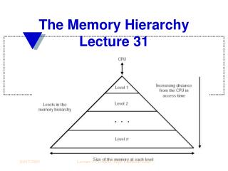
Processor Control Secondary Storage (Disk) Second Level Cache (SRAM) Main Memory (DRAM) On-Chip Cache Datapath Registers Compiler Hardware Fastest Speed: Operating System Slowest Size: Smallest Biggest Cost: Highest Lowest Main Memory • Main memory: I/O interface between caches and servers • dst of input & src of output
Main Memory Performance measures • Latency the time to retrieve the first word of the block important for caches; harder to reduce; • Bandwidth the time to retrieve the rest of this block important for multiprocessors, I/O, and caches with large block sizes; easier to improve with new organizations;
Main Memory Performance measures • Latency access time: the time between when a read is requested and when the desired word arrives; cycle time: the minimum time between unrelated requests to memory; or the minimum time between the start of on access and the start of the next access;
Main Memory • SRAM for cache • DRAM for main memory
SRAM • Static Random Access Memory • Six transistors per bit to prevent the information from being disturbed when read • Don’t need to refresh, so access time is very close to cycle time
DRAM • Dynamic Random Access Memory • Single transistor per bit • Reading destroys the information • Refresh periodically • cycle time > access time
DRAM • Dynamic Random Access Memory • Single transistor per bit • Reading destroys the information • Refresh periodically • cycle time > access time • DRAMs are commonly sold on small boards called DIMM (dual inline memory modules), typically containing 4 ~ 16 DRAMs
DRAM Organization • RAS: row access strobe • CAS: column access strobe
DRAM Improvement • Timing signals allow repeated accesses to the row buffer w/o another row access time; • Leverage spatial locality each array will buffer 1024 to 4096 bits for each access;
DRAM Improvement • Clock signal added to the DRAM interface, so that repeated transfers will not involve overhead to synchronize with memory controller; • SDRAM: synchronous DRAM
DRAM Improvement • Wider DRAM to overcome the problem of getting a wide stream of bits from memory without having to make the memory system too large as memory system density increased; widening the cache and memory widens memory bandwidth; e.g., 4-bit transfer mode up to 16-bit buses
DRAM Improvement • DDR: double data rate to increase bandwidth, transfer data on both the rising edge and falling edge of the DRAM clock signal, thereby doubling the peak data rate;