Download
1 / 19
190 likes | 336 Views
Status of the Front-End Electronics 5 June 2013 R . Chris Cuevas. Brief status update of DAQ/Trigger production hardware Firmware development for HPS application CLAS12 CTP ‘upgrade’ notes Summary . All Trigger Modules In Production . SSP. FADC250. CTP. SSP. GTP.

E N D
Status of the Front-End Electronics 5 June 2013 R. Chris Cuevas • Brief status update of DAQ/Trigger production hardware • Firmware development for HPS application • CLAS12 CTP ‘upgrade’ notes • Summary
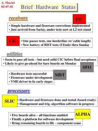
All Trigger Modules In Production SSP FADC250 CTP SSP GTP L1 Trigger ‘Data’ MTP Ribbon Fiber • Global Trigger Crate • Sub-System Processor • Global Trigger Processor SD TI TD Trigger ‘Link” Control Clock, Sync MTP Ribbon Fiber TS • Front End Crate • FADC250, (FADC125), (F1TDC) • Crate Trigger Processor • Signal Distribution • Trigger Interface • Trigger Control/Synchronization • Trigger Supervisor • Trigger Distribution 2
Hardware Status • All 726 VXS FADC250 boards have been received • -- There will be plenty of spare units for HPS • -- Overall production lot had ~10% of boards that did not pass initial • acceptance testing. These boards will be evaluated and repaired. • All Signal Distribution boards have been received and tested. • Trigger Interface boards have been received and tested. At least one TI unit will operate in Trigger Supervisor mode for HPS. • Hall D Crate Trigger Processor is in production. • -- Requirements for CLAS12 Trigger Processor have been defined • -- CLAS12 Trigger Processor will have upgrades that allow for new requirements defined for HPS cluster finding and other advanced triggering needs. (See Scott Kaneta’s talk for details) • Sub-System Processors have been received and tested by Ben. • -- Production SSP take advantage of a single FPGA to manage up to 8 front end crates and will communicate to new CLAS12 Trigger Processor at 5Gbps. 3
Present Flash ADC ImplementationEnergy Sum Trigger (Hall D application) CH-1 12 Bits 12 Bits VXS Gigabit serial Transfer rate of 4Gb/s* per board *(2 full duplex lanes @2.5Gb/s * 8/10b) Transfer 16-bit Energy Sum every 4ns Energy Sum 16 Channels To Crate Trigger Processor (VXS Switch Card) + Xilinx FPGA Trigger Function Pre-Processing APD Signals CH-16 CH-16 CH-1 Global Trigger Round Trip Latency <3us Energy & Time Algorithms VME Readout 8μs ADC Sample Pipeline 4
Technique for using channel sums and timing for cluster finding • 32ns ‘frame’ begins with SYNC • Each channel sum value is a selectable 5-bits of 20-bit sum • Common threshold register for all channels • Common registers for Number of Samples Before and After Threshold • NSA • NSB • If channel does not pass threshold transfer zero sum and clock bits • Retain existing FADC250 features for channel readout • -- Counters (scalers) for every channel • -- EPICs or CODA readout for scalers • Definitions of ‘framing’ technique for synchronous transfer of individual sum • for every channel • Methods for cluster finding algorithm defined for Crate Trigger Processor • Multi-crate cluster collection and final trigger Sub-System Processor HPS Test Run 5
Framing the Trigger Data from the FADC250 HPS Test Run 5 bit value extracted from Channel energy sums 3 timing bits used to encode 4ns clock for TOT sample time 16 Bytes every 32ns (5ADC + 3 timing bits) 1 Byte per channel HPS trigger process runs @4ns ‘Integrate’ over 4 frames Report every 128ns FADC250 retains functions for VME data readout of signals when system trigger is received For HPS a 13 bit value will be extracted for the channel energy sums. 3 bits will be used for timing encoding to resolve 4ns TOT. Requires 32bytes in 32ns so serial transfer speed must double to 5Gbps per lane 6
Implementation for encoding data to CTPHall B – HPS Test Run Implementation CH-1 12 Bits 12 Bits VXS Gigabit serial fabric Transfer rate of 4Gb/s per board (2 full duplex lanes @2.5Gb/s) Use 32ns ‘frame’ to Transfer 16-bytes Each channel is 1 byte: 5 bit Sum + 3 bits for timing To Crate Trigger Processor (VXS Switch Card) Xilinx FPGA Channel Sum Processing APD Signals CH-16 CH-1 3 bit clock encoding Allows 4ns clock recovery in 32ns ‘frame’ 16 Bytes in 32ns Meets the 4Gb/s transfer bandwidth Per board 32 ns CH-16 • The TDC algorithm feature of the FADC250 was removed to allow for the • HPS firmware modifications • The TDC feature provided 6-bits of resolution with 62.5ps LSB 7
Performance Summary(Updated since September Collaboration Meeting) • Successful implementation of full two crate FADC250 system for HPS spring 2011 test run! • FADC250 boards were not final production versions, but this was • the first time that a two crate system was installed and operated • in a beam experiment. Gigabit serial lanes @2.5Gb/s from all boards in two crates without any significant issues with VME 2eSST readout • The requirements for the new CLAS12 Trigger Processor include • 5Gbps links from each of the FADC250 boards for much higher charge resolution from each channel. The new information will be used for the Calorimeter cluster finding algorithm. • All issues identified during HPS Test Run have been documented and will be resolved. Need significant test time to verify 5Gbps requirement. 8
CLAS12 (HPS) Firmware Upgrade NotesNew FADC250 Firmware and New CTP Design CH-1 12 Bits 12 Bits VXS Gigabit serial fabric Transfer rate of 8Gb/s* per board *(2 full duplex lanes @5Gb/s =10Gb/s * 8/10b encoding) Use 32ns ‘frame’ to Transfer 16-bytes Each channel is 16 bit word: 13 bit Sum + 3 bits for timing To Crate Trigger Processor (VXS Switch Card) Xilinx FPGA Channel Sum Processing APD Signals CH-16 CH-1 • Existing CTP used close to 70% of FPGA resources • For HPS Test Run Trigger Application • CLAS12 will use CTP for three plane calorimeters • - PCAL, ECAL • - Possibility for more complex trigger algorithms • Proposal for CLAS12 wire chambers to use CTP • Output Fiber Transceiver will be upgraded • Requirements document complete • New hardware design 32 ns 3 bit clock encoding Allows 4ns clock recovery in 32ns ‘frame’ CH-16 32 Bytes in 32ns Will require that the FADC250 transfer bandwidth doubles to 8Gb/s 9
Design Goals for FADC250 Firmware and Trigger Boards • Double the transmission speed from FADC250 boards to CTP • Allows for higher energy resolution information from each channel • Allows for timing resolution of 4ns • Preliminary testing shows promising results with 5Gb/s per ‘lane’ • Must continue testing @5Gb/s with VME 2eSST bus activity to resolve issues • Restore the TDC function to FADC250 • -Will require firmware optimization and timing verification efforts • -Successful implementation would eliminate need for signal splitting, discriminators, TDC modules and additional Crates. • Add ‘coefficient’ (Gain) registers to be programmed for each FADC250 channel 10
Draft Activity Schedule for Two Quarters( June-13 January-14) 11
Design Goals for FADC250 Firmware and Trigger Boards • Double the transmission speed from FADC250 boards to CTP • Allows for higher energy resolution information from each channel • Allows for timing resolution of 4ns • Preliminary testing shows promising results with 5Gb/s per ‘lane’ • Must continue testing @5Gb/s with VME 2eSST bus activity to resolve issues • Restore the TDC function to FADC250 • -Will require firmware optimization and timing verification efforts • -Successful implementation would eliminate need for signal splitting, discriminators, TDC modules and additional Crates. • Add ‘coefficient’ (Gain) registers to be programmed for each FADC250 channel 12
Summary • ALL 12GeV pipelined DAq and Trigger custom electronic modules are in production with most designs completely tested and accepted. • Many detector groups are using FADC250 boards for testing and full crate performance testing is ongoing for each Hall Group. • New requirements for CLAS12 Trigger Processor have been completed and include all trigger processing ideas for each detector subsystem. Planned FPGA device will exceed requirement specification but will allow for future improvements of triggering applications. • Significant challenges remain and testing is crucial to verify that FADC250 boards will be reliable at the 5Gbps serial transmission rate. • Electronics group will support re-design work needed for Inner_Calorimeter circuit boards and any other electronic needs for the experiment. • Acknowledgement of continued significant hardware and firmware contributions from: • Hai Dong, Scott Kaneta, Nick Nganga, Ben Raydo, Ed Jastrzembski, and Bryan Moffit, William Gu 13
Backup Slides All sorts of good stuff
Successful HPS Beam Test with New 12GeV Cluster Finding Trigger App Two crate Trigger Signal From SSP to TI(TS) • HPS Test Run in Hall B used two full VXS crates • 432 APD channels 27 FADC250 • Cluster finding algorithm in Crate Trigger Processor -- Pushing the resource limit! • New firmware to encode individual channel sums • CTP firmware will report cluster centroid to SSP • SSP will create trigger from CTP output • Exploits the use of the 4Gb/s VXS bandwidth from each FADC250 module • New technique to report signal threshold crossing with 4ns resolution and 5bit amplitude for every channel • Experiment shows that Hall D L1 Energy Sum algorithm for Calorimetry will clearly ‘fit’ into CTP • Ebeam 5.55 GeV Radiator 10^-4 r.l. Au Collimator 6.4 mm Pair spectrometer convertor 1.8x10^-3, 4.5x10^-3 and 1.6x10^-2 r.l. Pair spectrometer field - -760A and +760A MTPFiber LINUX MTP Fiber CODA LINUX HPS DAq rates: Ecal +20KHz With Si Tracker: 4KHz 8
HPS Firmware Design – Implementation Brief History • 26-May-2011 HPS collaboration meeting • -- Initial ideas on what information was needed for HPS trigger • -- Existing stable firmware was designed for Hall D Energy sum • 18-Oct-2011 HPS collaboration meeting • -- Firmware requirements document created • -- Clear definition of what information was required for cluster finding • -- Methods were coded, simulated, and verified (FADC250) • -- Crate Trigger Processor firmware requirements defined • -- Sub-System Processor firmware requirements started • Nov-11->Feb-12 • --Pre-Production FADC250 units configured in a two crate • test station for full test of new trigger firmware • -- Test station includes Trigger Interface, Signal Distribution (Timing) • and CODA library development plus GUI • March-2012 • -- CTP cluster finding algorithm fine tuning and test with fully instrumented crates • 13-April-2012 • -- Installation of FADC250 and Trigger modules in Hall B • -- Cabling, debug, interface to APD electronics, TEST • 17-May-2012 • -- HPS test run with beam in Hall B! (Even the flooding could not stop this event) 2
Crate Trigger Processor Point of ViewCluster Finding with Energy Resolution/Channel 6 Bit Sum CE1 CH-1 Sub-System Processor CE0 Serial Stream 32 ns Board 1 6 Bit Sum CE1 CH-16 CE0 4 x 2.5Gb/s fiber links From crates to Sub-System Processor Final Cluster Algorithm To process all calorimeter channels Cluster Energy Trigger Will have much more resolution than initial DVCS implementation Crate Trigger Cluster Combiner 8Gb/s APD Signals 6 Bit Sum CE1 CH-1 CE0 Serial Stream Board 16 32 ns 6 Bit Sum CE1 CH-16 CE0 8Gb/s 11
Flash ADC Implementation To trigger logic Trigger Pulse Pre-Processing Capture Window Readout Energy & Time Algorithms Sample Clock Event #2 Event #1 detector signal FADC 8μs ADC Sample Pipeline Trigger #1 Trigger #2 Trigger Input • Sampling Flash ADC stores digitized signal in 8us memory • Trigger input copies a window of the pipeline and extract pulse charge and time for readout • Trigger output path contains detailed information useful for cluster finding, energy sum, etc. • Hardware algorithms provide a huge data reduction by reporting only time & energy • estimates for readout instead of raw samples 21
Flash ADC 250MHz Fast Electronics DAQ Groups 23-Sept-2011 • 16 Channel, 12-bit • 4ns continuous sampling • Input Ranges: 0.5V, 1.0V, 2.0V • (user selectable via jumpers) • Bipolar input, Full Offset Adj. • Intrinsic resolution – σ = 1.15 LSB. • 2eSST VME64x readout • Several modes for readout data format • Raw data • Pulse sum mode (Charge) • TDC algorithm for timing on LE • Multi-Gigabit serial data transport of trigger information through VXS fabric • On board trigger features • 16 Channel SUM every 4ns • Channel coincidence, Hit counters • Automatic Test Station is complete • Engineering Run – 40 Delivered! • 18 Hall D • 17 Hall B • Production Procurement FY12 • ~ 700 Boards for all Halls 2