Download
1 / 19
200 likes | 339 Views
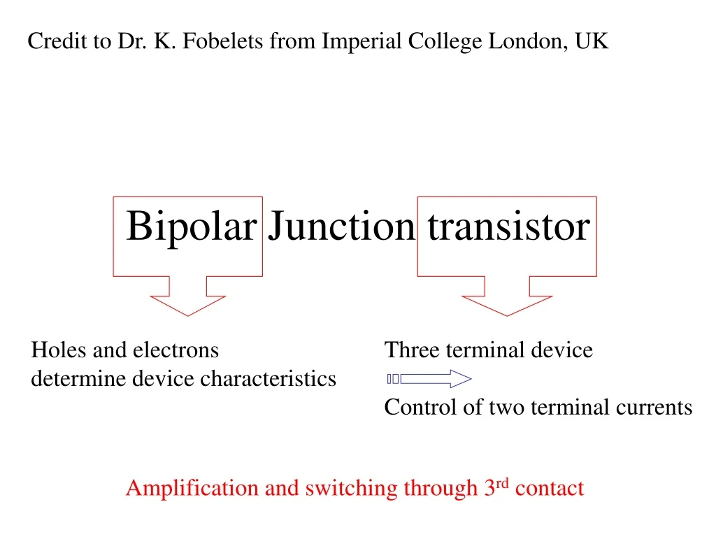
This educational text explores the fundamental principles behind bipolar junction transistors and their operation. It covers topics such as holes and electrons determining device characteristics, control of two terminal currents, and amplification through a third contact. Credit to Dr. K. Fobelets from Imperial College London, UK. The text delves into the intricacies of bipolar junction transistors, discussing recombination, carrier flow, amplification factors, base transport, and current calculations in pn junctions. It also explains carrier dynamics, current distributions, and key parameters affecting transistor performance. This resource offers a comprehensive insight into the operation and behavior of bipolar junction transistors.

E N D
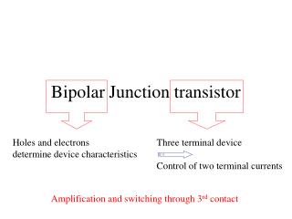
Holes and electrons determine device characteristics Three terminal device Control of two terminal currents Credit to Dr. K. Fobelets from Imperial College London, UK Bipolar Junction transistor Amplification and switching through 3rd contact
E B C IE IC p+ n p holes e- gain, reverse bias holes IE IC ICB0 I’B I”B Recombination e- loss e- loss, forward bias IB Carrier flow in BJTs IB IB = I’B + I”B – ICB0
Electrostatically neutral h+ e- tp recombine with Wb << Lp Control by base current : ideal case. Based upon space charge neutrality Base region IE = Ip tt transit time tt < tp Based on the given timescales, holes can pass through the narrow base before a supplied electron recombines with one hole: ic/ib = tp/tt The electron supply from the base contact controls the forward bias to ensure charge neutrality!
E IC IEp B equilibrium Injection of carriers e- VBE>0 Wb < Lp x h+ No amplification! IEn Amplification! How good is the transistor? C • IEp>>IEn • Wish list: or g = IEp/(IEn + IEp) ≈ 1 g: emitter injection efficiency • IC≈ IEp or B= IC/IEp≈ 1 B: base transport factor or a= IC/IE≈ 1 a: current transfer ratio + (1-B) IEp • IB≈IEn thus b= IC/IB= a/(1-a) b: current amplification factor ICB0 ignored
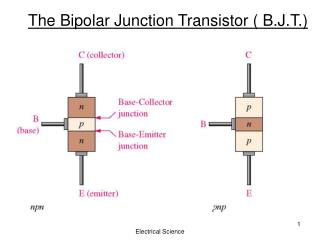
Forward biased p+n junction is a hole injector Reverse biased np junction is a hole collector B E W < Lp Review 1 – BJT basics IC Forward active mode (ON) IE VBC V V VBC I I EB E C p+ n p C E
Forward biased p+n junction is a hole injector Reverse biased np junction is a hole collector B E W < Lp Review 1 – BJT basics IC Forward active mode (ON) IE VBC V V VBC IB=I’B +I”B I I EB E C p+ n p C E
IB = I’B + I”B – ICB0 Review 2 Amplification? Recombination only case: I’B, ICB0negligible ic/ib = tp/tt Carriers supplied by the base current stay much longer in the base: tp than the carriers supplied by the emitter and travelling through the base: tt. b = tp/tt But in more realistic case: I’Bis not negligible b = IC/IB With IB electrons supplied by base = I’B = In IC holes collected by the collector = Ip
Currents? • In order to calculate currents in pn junctions, knowledge of the variation of the minority carrier concentration is required in each layer. • The current flowing through the base will be determined by the excess carrier distribution in the base region. • Simple to calculate when the short diode approximation is used: this means linear variations of the minority carrier distributions in all regions of the transistor. (recombination neglected) • Complex when recombination in the base is also taken into account: then exponential based minority carrier concentration in base.
E B C p(x) B DpE Without recombination pn0 With recombination pn0 DpC x 0 Wb Minority carrier distribution • Emitter injects majority carriers into base. • dpn(0)=pno (exp(VEB/VT)-1) • Assume active mode: VEB>0 & VBC<0 • Collector collects minority carriers from base. • dpn(Wb)=pno (exp(VBC/VT)-1) dp(x) 0
dp(x) B DpE DpC x 0 Wb See expressions for diode current for short diode Currents: simplified case • Then IE = total current crossing the base-emitter junction Assume I”B=0 & IBC0= 0 • Then IC = IEp gradient of excess hole concentration in the base • IB without recombination is the loss of electrons via the BE junction: I’B • Then IB = gradient of excess electron concentration in the emitter
dp(x) DpE Linear variation of excess carrier concentration: DpC x 0 Wb Narrow base: no recombination: Ip →minority carrierdensity gradient in the base DpE = pn0(e eVEB/kT – 1) ≈pn0 e eVEB/kT DpC = pn0(e –e|VBC|/kT – 1) ≈ -pn0 Note: no recombination
Diffusion current: Collector current: Ip Hole current: Collector current No recombination, thus all injected holes across the BE junction are collected. Base current??
dn(x) Dnp Linear variation of excess carrier concentration: 0 x xe 0 Look at emitter: In → minority carrier density gradient in the emitter Dnp = np0(e eVEB/kT – 1) ≈np0 e eVEB/kT
Diffusion current: Base current: In Base current: The base contact has to re-supply only the electrons that are escaping from the base via the base-emitter junction since no recombination I”B=0 and no reverse bias electron injection into base ICB0=0.
Emitter current: Current gain: Emitter current The emitter current is the total current flowing through the base emitter contact since IE=IC+IB (current continuity)
VBC BE E C p+ n p C E B Original base width V V I I Depletion width changes with VBC Effective base width Metallurgic junction Non-ideal effects in BJTs • Base width modulation
base width modulated VA Base width modulation • Early voltage: VA iC Wb ideal IB -vCE
Conclusions • Characteristics of bipolar transistors are based on diffusion of minority carriers in the base. • Diffusion is based on excess carrier concentrations: • dp(x) • The base of the BJT is very small: • dp(x) = C1 ex/Lp + C2 e-x/Lp • Base width modulation changes output impedance of BJT.